Category: Ai
Posts
read more
Chatting with Schematic: Evaluation of LLMs' Know-How in Electronics
This article evaluates the proficiency of 11 contemporary Large Language Models (LLMs) in performing electronic circuit analysis.
Utilizing OpenCode, an open-source agentic framework, the LLMs are tasked with analyzing a clock generator’s resistor-capacitor (RC) network defined in a KiCad 9.0 schematic. To facilitate LLMs’ comprehension, an efficient preprocessing methodology is introduced to convert schematic data into structured CSV formats. The evaluation requires the models to parse circuit netlists, retrieve specifications from component datasheets available in the workspace, and calculate the critical circuit parameters, specifically the common-mode voltage and differential swing of the clock output.
Category: Fpga
Posts
read more
Test-Board from PCBWAY has Arrived!
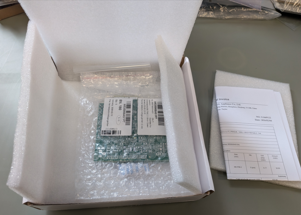
Some days ago I ordered a testing PCB from PCBWAY, and today the package has arrived!

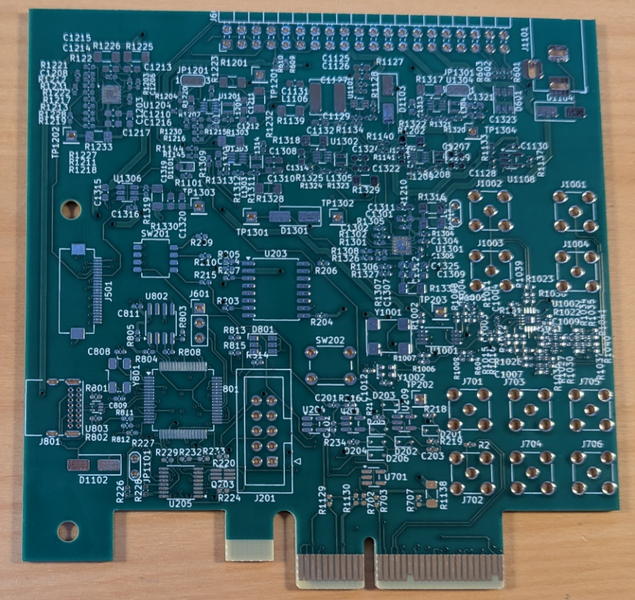
FRONT:
BACK:
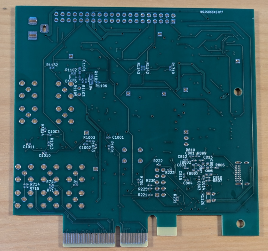
As discussed in the previous article, this is a test-board for the future PCIe card with Agilex 3 FPGA. But presently - no FPGA. The board combines several power supplies (dc/dc converters), clock generator with level shifters, reset, and USB-JTAG:

Posts
read more
Practical AI in HW Development: Importing BGA Pad-to-Die Lengths from Excel to Kicad Footprint
In hardware design, tedious manual data entry is a common bottleneck. I recently explored how the ‘AI revolution’ - specifically LLMs and GitHub Copilot - could automate a specific, repetitive task: importing BGA pad-to-die lengths into KiCad 9. The input Excel table, downloaded from Altera site, has around 270 rows, so the motivation to not do the import by manually entering numbers into software was pretty high.
What is the Pad-to-Die Length
The picture bellow shows a cross section of a typical integrated chip in a BGA package. Balls at the bottom are soldered to the PCB, while the actual IC silicon die is much smaller and sits on a ceramic substrate. The substrate acts as an intermediary routing layer, connecting the silicon die to the BGA balls. The traces between balls to the die are not the same length. The pad-to-die length, or package length, is the length of the internal trace in the package; it is different for every pad or ball (unless the IC designer takes care to do the package delay matching).
Posts
read more
AGILA, and Her Test-board
AGILA will be a new open-source board with the Altera Agilex 3 FPGA, 2 GB to 8 GB
of LPDDR4 RAM and the PCI-Express interface. The Agilex 3 FPGA includes hard-IP support for PCI- Express interface up to Gen3 x4 and the LPDDR4 x32 up to 1066MHz (2133MT/s). The board form factor will be a low-profile PCI-Express card with the x4 edge connector. The upper edge of the board will be occupied by extension pin-header connectors. The board will also include a JTAG port and USB/JTAG interface for easy HDL development.
Posts
read more
Powering the Agilex 3 FPGA
The picture below is an extract from Power-Supply Block Diagram of the official Agilex 3 Devkit. The FPGA requires multiple power supply levels: from 0.75V to 3.3V. Specification is found in altera document Power Management User Guide: Agilex™ 3 FPGAs and SoCs and details for particular device in Agilex™ 3 FPGAs and SoCs Device Data Sheet.
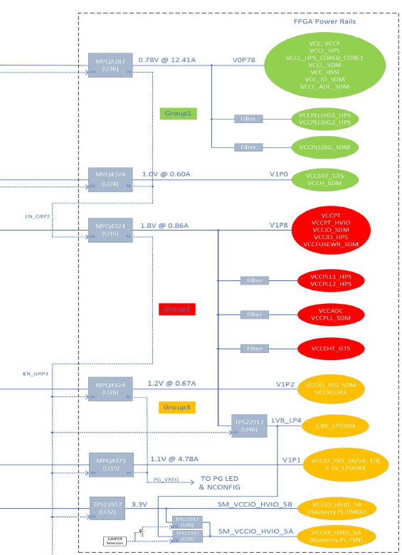
Minimum Set of Power Levels
This is the list of mandatory power supply levels needed for the Agilex 3 FPGA:
Posts
read more
Clocking the Agilex 3 FPGA
Theoretically, Agilex 3 FPGA does not require any external clock signals to load bitstream and to operate an (asynchronous) user design. However, in practice, all designs will need to supply some clock signals for use in EMIF (e.g. LPDDR4) or GTS (e.g. PCIe) and other integrated IP. To be specific in this post, we focus on clocking scheme of the Agilex 3 Devkit board (block diagram pictured below).

Secure Device Manager (SDM)
Secure Device Manager (SDM) is responsible for booting the FPGA: loading of bitstream (typically from QSPI-Flash), array configuration and HPS boot. Although the SDM can operate from an internal free-running clock, an external (more stable) clock is necessary in case the design is using EMIF (LPDDR4) or GTS (PCIe). The external clock should be 25MHz, or 100MHz or 125MHz at 1.8V-level single-ended LVCMOS and must be fed into the dedicated pin OSC_CLK_1 (AG11). The expected frequency is pre-configured in the header part of the bitream (bitstream header, up to 512kB, is always loaded with internal clock, but the rest of the loading/booting process is configurable in the header). In case of the Agilex 3 Devkit design the 100MHz clock for SDM is generated in a dedicated external oscillator Skyworks 510KBB100M000CAG (Mouser).
Posts
read more
Bitstream Loading in Agilex 3 FPGA
Agilex 3 FPGA supports loading of the configuration bitstream by multiple methods. A method is selected by 3 strapping pins MSEL[2:0] (these are multi-purpose strapping pins). The common methods are:
-
MSEL[2:0]=111 => wait for JTAG download,
-
MSEL[2:0]=011 => normal QSPI Flash download mode
-
MSEL[2:0]=001 => “fast” QSPI Flash download mode - this just skips a 10ms wait before accessing QSPI flash which is normally part of the normal QSPI flash download mode. This could help with PCIe link-up requirements, but the design must ensure that the QSPI device is ready.
Posts
read more
GTS Transceivers with PCI-Express hard-IP in Agilex 3
Agilex 3 FPGA supports PCI-Express via its four GTS transceiver links. Each GTS physical link (tx+rx) supports up to 12.5Gbps transfer speed. On top of the GTS transceivers the FPGA implements hardened IPs for PCI-Express 3.0 x1-x2-x4, Ethernet 10 Gbe link, and USB 3.0 (only with HPS).
Available PCI-Express Throughput
PCI-Express speed is specified in generations: from 1.0 to 8.0 (planned in 2028), and in port width: from x1 to x16. The table below, copied from wikipedia, shows the expected throughput for the given generation and port width:
Posts
read more
LPDDR4 in Agilex 3 FPGA
Presently (2025) there are two perspective busses for connecting DRAM devices in embedded systems:
-
DDR3L
-
LPDDR4 (and its lower-power variant LPDDR4X)
The DDR3L supports traditional DDR multidrop bus topology with VTT termination and multiple memory devices sharing the address/control bus. The LPDDR4 is a completely different protocol and allows just a single memory device attached to the controller, with the advantage that external termination not required (saving board space and power).
Posts
read more
Could we design an FPGA-based compute accelerator on an M.2 card?
Ever since I attended the Altera FPGA workshMicronop featuring their new Agilex 3 device, I am thinking if Agilex could be the right FPGA to implement a general-purpose computation accelerator (i.e. a GPU) with a fast PCI-Express interface and a significant amount of DDR DRAM memory.
The following features of Agilex 3 FPGAs are notable in the context:
-
100k to 135k logic elements in the two largest variants
-
affordable cost of a device around 130 USD/piece
Posts
read more
AXC3000: Agilex FPGA Starter Kit
Recently I attended Arrow’s Agilex 3 FPGA workshop, which promoted, obviously, the new Altera Agilex 3 FPGAs. In the workshop we completed lab tasks using also the new AXC3000 Starter Kit that features the Agilex 3 FPGA. At the end of the day there was a quiz and so I happened to win one the AXC3000 boards for myself. In this article I present my first-look analysis of the board.

Category: X65
Posts
read more
Beware of Non-Legit Indiegogo Campaigns
There is an ongoing Indiegogo campaign called “X65GS 65816 Gaming Console”, see screenshot below.
I - as the creator of the x65 project - do not support and do not endorse this campaign.
In the campaign page they reused my own ‘amateur’ photos of that one x65-sbc device, which is right now on my work-desk at home. IT MEANS: they do not have the capacity or knowledge to produce own replicas of the x65-sbc computer for testing and marketing purposes, yet they have the guts to request money from unsuspecting customers!
Posts
read more
New x65 Debugger in the textual Framework
I started a new debugger tool for my x65 project. Previously I created a dozen of single-purpose python scripts (running on a linux PC) that let me single-step the CPU, read CPU registers, dump memory and so on. The scripts use a common ‘backend’ modules to connect to the x65 hardware over the USB / FTDI interface, but otherwise each script acts on its own.
These python scripts and modules are located in the project subdirectory x65pyhost:
Posts
read more
Enclosure for X65
I designed an enclosure box for the x65-SBC computer. For modelling I used Siemens Solid Edge 2024 CAD software, of which I have the Employee Edition. (I think it is just similar to the free Community Edition, but I did not verify.)

The enclosure box is composed of ’top’ and ‘bottom’ parts which can be 3d-printed individually. The parts are screwed together with four M3x25 screws and M3 nuts, with the PCB held in the middle:
Posts
read more
Dreamtracker's Rabbit Hole
As mentioned in previous post, Matej asked me if Dreamtracker app is running on X65. I told him that yes, it should run, but better to test it first myself. I downloaded Dreamtracker in its current version V0.71, fired it up, and well, after a promising start - I could see its main menu for a split second - the program crashed into the Monitor…. Well, that felt embarrasing :o
This youtube video shows the crashed start:
Posts
read more
The X65 Saga Continues
It’s Autumn again and I am revisiting my Project X65. My list of to-do tasks is endless and growing still :-)
-
finishing tests of the A1 prototype
-
load BOM to Mouser
-
testing the USB interface
-
better ESD concept
-
indication of stopped CPU
-
consider new extension connector
-
consider if SDMMC power should be switched
-
feasibility of machine assembly of prototypes
-
check the new SMC code in CX16
-
check the new 65816 code in CX16
Posts
read more
X65-SBC Video-Terminal for the Forth OF816 Interpreter
In the previous post I have mentioned that I am working on a port of the 32-bit Forth interpreter OF816 to my X65-SBC, an 8/16-bit retro computer that I am building. The software runs on the X65-SBC in the 65C816 processor, but the user textual input and output was so far realized via the USB/UART interface terminated on a host PC in a terminal emulator (e.g. putty).
As the next logical step, shown in the demo below, I have implemented a video text terminal using the VERA chip and the VGA output from the X65-SBC. VERA is the computer’s video chip implemented in an FPGA. VERA has 128kB of internal VRAM and could be configured in various graphics modes, typically generating a 640x480-pixel resolution screen. For the purpose of a textual terminal output I am configuring VERA to display 80 columns by 60 rows of visible characters. Each character is 8x8 pixels, and each character can have one of the 16 foreground and background colors.
Posts
read more
32-bit Forth for the X65 with 65C816 CPU
I am working on a port of the 32-bit FORTH interpreter OF816 for my X65-SBC computer with the 65C816 CPU. The OF816 was created by mgcaret and is available on github. I made a fork of the OF816 project and added a new branch for my work: x65-sbc.
The OF816 already supports a couple of 65C816-based systems: GoSXB, Apple IIgs, Neon816 and the W65C816SXB. I added a new subdirectory X65 in the platforms directory and initially copied from the Neon816 port, because it seemed the simplest.
Posts
read more
Reading of 6502/65816 CPU Registers by a PC-based Debugger
Modern microcontrollers and microprocessors have built-in facilities for external debuggers to read/write registers, set breakpoints and generally fully control the CPU. This is one of the main usecases of the standard JTAG interface. The 6502 and 65816 CPUs were created more than a decade before the first version of JTAG was even defined. They contain no support for external debuggers whatsoever.
To overcome the lack of debugger support, the system bus controller “NORA” in the X65 computer (link to GIT repository; photo below) implements the necessary functions for a debugger running on a host PC (with Linux or Windows) and connected over the USB-C port. With this support in NORA a debugger can control the 6502/65816 CPU at the instruction level.
Posts
read more
Single-Board version of X65, now on Hackaday
In the last 2 months I have re-done my X65 double-decker computer into a Single Board Computer (SBC).
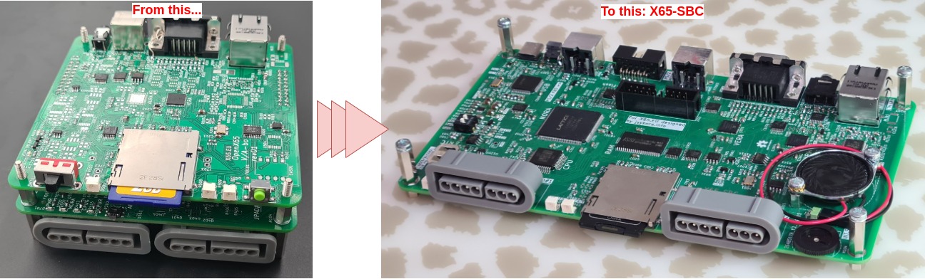
The single-board version fixes some of the electrical problems I had on the first version and it has way better signal integrity thanks to the 4-layer PCB. Other than that, the feature-set is basically identical.
-
added the mono speaker with volume control.
-
added (Olimex) UEXT connector - 2x5 pins connected to the NORA FPGA.
Posts
read more
Differences between the 65C02 and 65C816 Processors in 8-bit Mode
In X65 the assembled CPU is either the 8-bit W65C02S or 16-bit W65C816S. The W65C816S is (partially) compatible with W65C02S. This page summarizes the differences from the low-level hardware point of view and in the case that the 65C816 is running in the 8-bit Emulation Mode.
These two photos shows the processors assembled on X65 main board:


Processor Pinout Comparison
Both processors are available in the same QFP-44 package, so they could be assembled alternatively on the same PCB.
Posts
read more
AURA FPGA: The replacement of YM2151
This document discusses the FM sound synthesis in the Commander X16 and in my x65 computer.
Sound in Commander X16
Sound in Commander X16 is generated by two sources that are mixed together:
1) by the Programmable Sound Generator (PSG) in VERA FPGA, and
- by the MIDI FM-synthesis chip YM2151.
The following picture is a block diagram of the sound subsystem in C’X16:

The PSG in VERA FPGA is a stereo sound generator loosely based on SID. It supports 16 channels (voices) and PCM playback. There is no ADSR or filters. This must be provided by software. The PSG is an integral part of VERA FPGA user logic that also generates the VGA video output. MIDI-like sound synthesis is provided by YM2151. Yamaha called it an FM operator Type-M (OPM). This is how the chip looked like:
Posts
read more
SNES Controller Mess
SNES Controllers typically look like this:

SNES controller is a cheap and easy way how to add a joystick interface to a DIY project. One controller can be cheaply had from aliexpress or similar for around 2 USD.
The controller has just 12 digital (on/off) buttons organized in various patterns, as you see in the photo: D-pad, ABXY buttons, two shoulder buttons, start and select. There are no analog interfaces, no LEDs etc.
Posts
read more
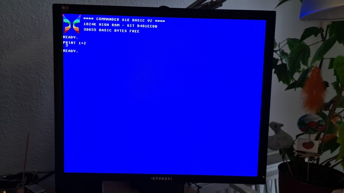
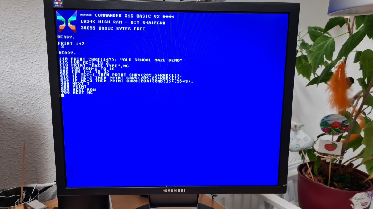
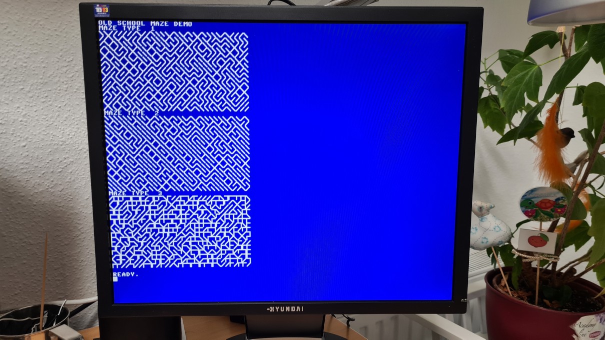
Milestone: X16 ROM BASIC runs the first program!
My Open-X65 project achieved a milestone: the unmodified X16 ROM can be loaded and runs! I manually typed in a BASIC maze program, which draws some ASCI graphics:
Posts
read more
Open-X65 GIT Repository
The Open-X65 GIT repository is now public:
Note: this is not a release! The project is very much a work-in-progress. You have been warned ;-)
Posts
read more
OpenX65 part-way assembled
Since the first post a lot of happened:
-
Motherboard PCB (bottom) has arrived, it is now part-way assembled with components and working quite well. First test-SW (a few instructions in a loop) is running OK.
-
I designed the second PCB (top) with video (VERA), audio (AURA - FM synth) and ethernet port. This was also manufactured, part-way assembled and now I have the first VGA video output.
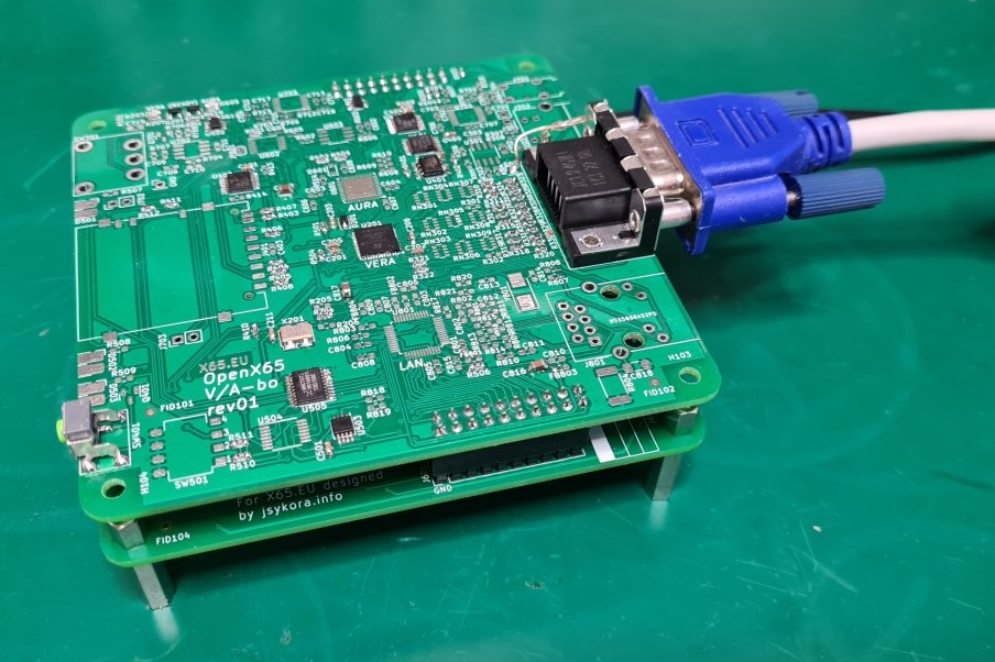
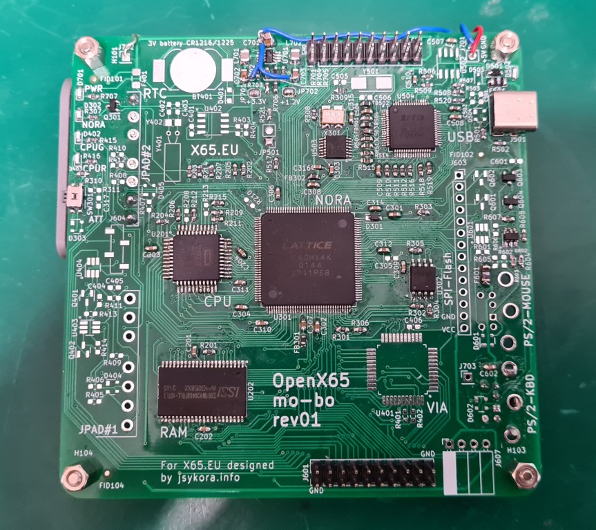
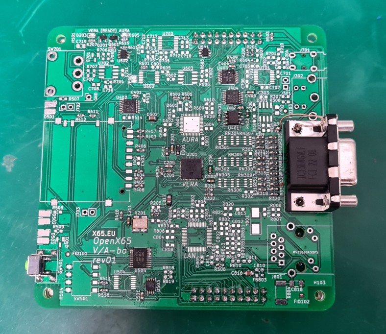
Posts
read more
My new 65C02-based retro-computer: OpenX65
I am starting a new hobby project called X65: I intend to create an open-source computer based on the “vintage” 6502 processor, which is still in production as the W65C02. The original 6502 was used in many home personal computers of the ’80s: Commodore, Atari, Apple II and so on. My computer will be called OpenX65.
Features as planned:
-
use W65C02 and (optionally) W65C816 (the 16-bit version) CPU
-
software compatibility with the Commander X16: a modern retro computer, developped by the 8-bit Guy
Category: Displays
Posts
read more
Linux 6.7.x on AMD GPU RX570 requires the kernel parameter amdgpu.dc=0
Symptoms: Running Fedora 38 and 39 with kernels 6.7.7 on AMD Ryzen 5 with AMD GPU RX570 (Sapphire Radeon PULSE ITX RX 570 4GD5, 4GB GDDR5) sometimes results in a blank screen (no video signal, monitor going to sleep mode) after the boot. The display manager (sddm, wayland) does not start (or is not visible, there is no video) and it is not possible to login or switch to a virtual console.
Posts
read more
Framebuffer Drawing with u8glib [VIDEO]
GDE021A1 is a graphics display with a resolution 172x72 pixels, each pixel is 2 bits deep (4 shades of grey). The display has an internal controller SSD1606 with a framebuffer. The framebuffer size is 172*72*2/8=3096 Bytes. When the display is powered up, the system processor sends initialization sequence that first sets up controller’s internal registers (the controller SSD1606 is fairly generic) and then sends new framebuffer content. The display controller then autonomously pushes the framebuffer contents to the physical screen.
The display controller can be configured to orient the framebuffer almost any way. I configured it into a landscape mode, with the X-axis going right and the Y-axis down, as shown on the photo.
Posts
read more
Mailbag: ePaper Display Module
Look what I’ve got by post today from our Chinese comrades at ‘Good Display’ factory: a nice small 2.04-inch electrophoretic display (EPD), or better known as ePaper/eInk display or ’electronic paper’.
[caption id=“attachment_232” align=“alignnone” width=“856”]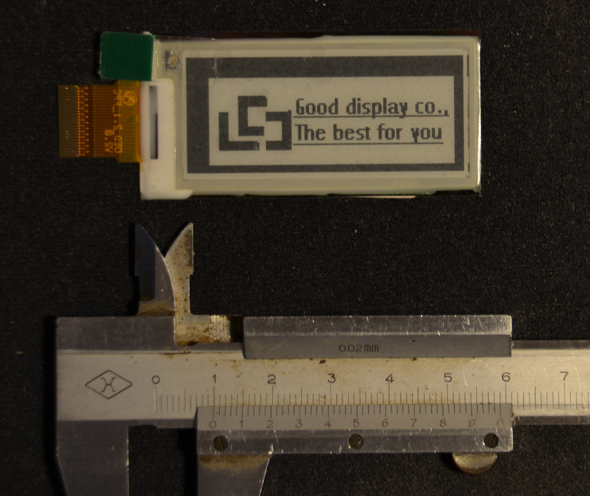 ePaper EPD display front side view[/caption]
[caption id=“attachment_231” align=“aligncenter” width=“632”]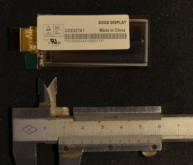 ePaper EPD display back side[/caption]
Electrophoretic displays (EPD) do not require any power to retain an image. Power is needed only when redrawing the screen. The technology is thus used in electronic paper readers such as Amazon Kindle or the Pebble smartwatch (correction: Pebble uses different display: Memory LCD).
Category: Highertech
Posts
read more
Did you know: Unaligned accesses in ARM
The X86 has always supported unaligned accesses. In the ARM world the first architecture that supported unaligned accesses in hardware was ARMv6. The architecture was implemented in the ARM11 core around the year 2002 and onward. There is an excellent article at ARM Infocenter giving technical details:
http://infocenter.arm.com/help/index.jsp?topic=/com.arm.doc.faqs/ka15414.html
The support for unaligned accesses must be enabled in an ARM core explicitly. This is done by setting the bit A in the register SCTLR. Still, unaligned accesses will be allowed only on Normal memory; accesses to Device memory type are always checked and will throw exceptions on misaligned accesses.
Posts
read more
Connecting MCU and FPGA at 100Mbit/s Using Ethernet RMII [Part 2]
This is Part 2 of a two-part series on Ethernet RMII. In Part 1 I described my hardware setup and basic Ethernet operation. In the second and final part I will describe the design of specialized MAC cores I implemented on FPGA, and there will be measurements to see how much throughput and latency the system can achieve.
Posts
read more
Connecting MCU and FPGA at 100Mbit/s Using Ethernet RMII [Part 1]
This is Part 1 of the two-part series on Ethernet RMII. Part 2 is also available.
Imagine your application requires a non-standard periphery controlled by an embedded processor. What options do you have? The periphery can be implemented in an FPGA; depending on periphery complexity you can choose an optimal FPGA that fits your budget. Where the processor goes? There are three possibilities: (a) inside FPGA as a soft-core → it will increase the cost of FPGA (larger type needed) and complicate HDL and software design. Or (b) inside FPGA as a hard-core → a nice compact solution and quite possible with heterogeneous FPGA from Xilinx (Zynq) and Altera (SoC). But the cost of these modern devices could still be too high for price sensitive applications. You must fit both your software and HDL to pre-engineered combinations of FPGA and ARM CPU sizes (perhaps a small Cortex-M core would suffice but you must pay for a gigahertz-class Cortex A cores).
The third option (c) is using a stand-alone MCU (maybe even not an ARM) and a standard FPGA. How do you connect them? You are limited to interfaces offered by the MCU. In modern low-end MCUs (by that I mean smaller STM32Fxxx devices) you have I2C (400 kbit/s), UART (115 kbit/s), SPI (~10Mbit/s), Fast Ethernet (100 Mbit/s). So what about the Ethernet core in the MCU? Could it be used to interface with FPGA? Sure it can!
Posts
read more
[Pic] BGA Dead-Bug Style
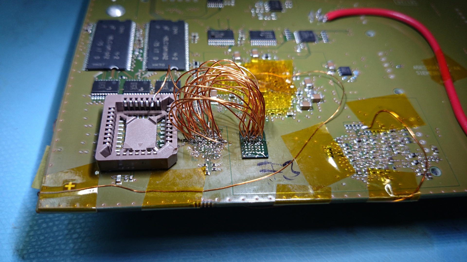 [half-way through; click a pic to see hi-res]
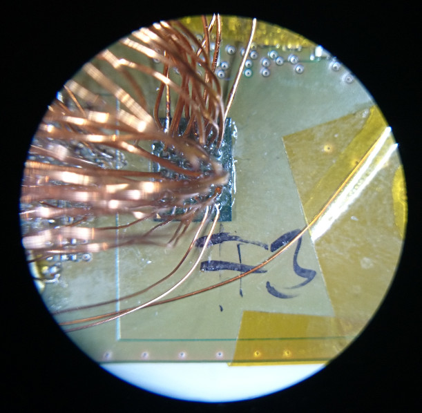 [connections to bga]
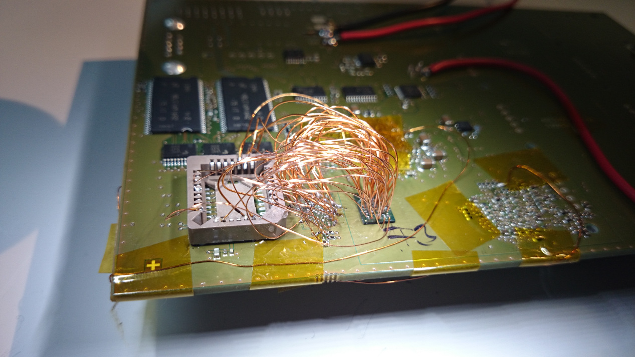 [finished “product”]
And it (almost) worked! Though not at-speed, because of wire inductances.
Posts
read more
ZedBoard: Late Xmas present has arrived!
Finally, after much waiting, my ZedBoard arrived on Tuesday. See it shining in the picture above, isn’t it lovely?
So far I managed only to unbox it and turn it on… Hence only a few notes on the beginnings:
- Running Vivado 2013.3 in Fedora Linux: see my previous post.
- Running the demo Linux bitstream from the supplied SD card: you need to reconfigure switches, at least JP8, JP9 should be at 3V3 side. Best to see the README on the SD card. The default configuration (JP7-11 at GND) is for JTAG download.
- Installing USB-JTAG cable drivers in Linux: surprisingly, all I needed to do was to run Vivado/2013.3/data/xicom/cable_drivers/lin64/digilent/digilent.adept.runtime_2.14.3-x86_64/install.sh as root.
- Missing impact tool in Vivado 2013.3: impact is deprecated. Use Hardware Manager / Open Target tabs in Vivado GUI.
Category: Ethernet
Posts
read more
Connecting MCU and FPGA at 100Mbit/s Using Ethernet RMII [Part 2]
This is Part 2 of a two-part series on Ethernet RMII. In Part 1 I described my hardware setup and basic Ethernet operation. In the second and final part I will describe the design of specialized MAC cores I implemented on FPGA, and there will be measurements to see how much throughput and latency the system can achieve.
Category: Zed
Posts
read more
Connecting MCU and FPGA at 100Mbit/s Using Ethernet RMII [Part 2]
This is Part 2 of a two-part series on Ethernet RMII. In Part 1 I described my hardware setup and basic Ethernet operation. In the second and final part I will describe the design of specialized MAC cores I implemented on FPGA, and there will be measurements to see how much throughput and latency the system can achieve.
Posts
read more
Connecting MCU and FPGA at 100Mbit/s Using Ethernet RMII [Part 1]
This is Part 1 of the two-part series on Ethernet RMII. Part 2 is also available.
Imagine your application requires a non-standard periphery controlled by an embedded processor. What options do you have? The periphery can be implemented in an FPGA; depending on periphery complexity you can choose an optimal FPGA that fits your budget. Where the processor goes? There are three possibilities: (a) inside FPGA as a soft-core → it will increase the cost of FPGA (larger type needed) and complicate HDL and software design. Or (b) inside FPGA as a hard-core → a nice compact solution and quite possible with heterogeneous FPGA from Xilinx (Zynq) and Altera (SoC). But the cost of these modern devices could still be too high for price sensitive applications. You must fit both your software and HDL to pre-engineered combinations of FPGA and ARM CPU sizes (perhaps a small Cortex-M core would suffice but you must pay for a gigahertz-class Cortex A cores).
The third option (c) is using a stand-alone MCU (maybe even not an ARM) and a standard FPGA. How do you connect them? You are limited to interfaces offered by the MCU. In modern low-end MCUs (by that I mean smaller STM32Fxxx devices) you have I2C (400 kbit/s), UART (115 kbit/s), SPI (~10Mbit/s), Fast Ethernet (100 Mbit/s). So what about the Ethernet core in the MCU? Could it be used to interface with FPGA? Sure it can!
Posts
read more
ZedBoard: Late Xmas present has arrived!
Finally, after much waiting, my ZedBoard arrived on Tuesday. See it shining in the picture above, isn’t it lovely?
So far I managed only to unbox it and turn it on… Hence only a few notes on the beginnings:
- Running Vivado 2013.3 in Fedora Linux: see my previous post.
- Running the demo Linux bitstream from the supplied SD card: you need to reconfigure switches, at least JP8, JP9 should be at 3V3 side. Best to see the README on the SD card. The default configuration (JP7-11 at GND) is for JTAG download.
- Installing USB-JTAG cable drivers in Linux: surprisingly, all I needed to do was to run Vivado/2013.3/data/xicom/cable_drivers/lin64/digilent/digilent.adept.runtime_2.14.3-x86_64/install.sh as root.
- Missing impact tool in Vivado 2013.3: impact is deprecated. Use Hardware Manager / Open Target tabs in Vivado GUI.
Posts
read more
Xilinx Vivado 2013.3 on Fedora 18: Working around a D-Bus bug
Running Xilinx Vivado 2013.3 (webpack license) on Fedora 18 may fail with the following error message:
$ vivado

****** Vivado v2013.3 (64-bit)
  **** SW Build 329390 on Wed Oct 16 18:26:55 MDT 2013
  **** IP Build 192953 on Wed Oct 16 08:44:02 MDT 2013
    ** Copyright 1986-1999, 2001-2013 Xilinx, Inc. All Rights Reserved.

INFO: [Common 17-78] Attempting to get a license: Implementation
process 17688: arguments to dbus_move_error() were incorrect, assertion "(dest) == NULL || !dbus_error_is_set ((dest))" failed in file dbus-errors.c line 282.
This is normally a bug in some application using the D-Bus library.
  D-Bus not built with -rdynamic so unable to print a backtrace
Abnormal program termination (6)
Please check '/home/jara/hdl/hs_err_pid17688.log' for details
The workaround is to make the D-Bus communication socket file /var/run/dbus/system_bus_socket unavailable when the Xilinx tools run.
Category: Cad
Posts
read more
How to: Altium Circuit Maker PCB to OSH-Park
How to export PCB design from the free Altium Circuit Maker v1.0.4 so that it can be submitted to OSH Park fab. This took me an evening to figure out; OSH Park service was bitching about missing “outline” and/or drill files.
Category: Video
Posts
read more
Framebuffer Drawing with u8glib [VIDEO]
GDE021A1 is a graphics display with a resolution 172x72 pixels, each pixel is 2 bits deep (4 shades of grey). The display has an internal controller SSD1606 with a framebuffer. The framebuffer size is 172*72*2/8=3096 Bytes. When the display is powered up, the system processor sends initialization sequence that first sets up controller’s internal registers (the controller SSD1606 is fairly generic) and then sends new framebuffer content. The display controller then autonomously pushes the framebuffer contents to the physical screen.
The display controller can be configured to orient the framebuffer almost any way. I configured it into a landscape mode, with the X-axis going right and the Y-axis down, as shown on the photo.
Posts
read more
EPD Display Working!
Today I have managed to get the GDE021A1 ePaper display (EPD) working! I used my minimal EPD-Driver board, which implements a flat-flex cable connector and a booster circuit for the display. The booster generates high voltages needed for display operation (around +-25V). The display is driven by STM32F101 Cortex-M3 CPU, mounted on a universal PCB. The picture below depicts my workbench setup (click to see a full-size image):
[caption id=“attachment_410” align=“aligncenter” width=“1205”]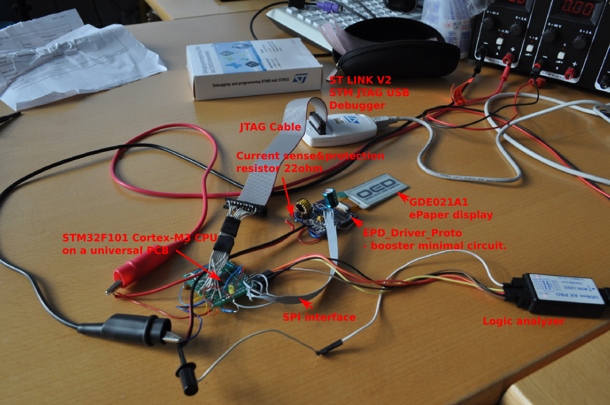 EPD Driver Prototype-workbench view with captions[/caption]
Category: Pip-Watch
Posts
read more
Error: jtag status contains invalid mode value - communication failure = SOLVED!
This issue bugged me a long time, finally I solved it this evening. Debugging code on my PIP-Watch using my ST-LINK-v2 JTAG debugger was very painful because the debugger software – OpenOCD and GDB – kept failing randomly during debug sessions with a rather cryptic message:
Error: jtag status contains invalid mode value - communication failure
Polling target stm32f1x.cpu failed, GDB will be halted. Polling again in 100ms
I scratched my head, updated firmware in ST-Link, looked at JTAG/SWDIO signals using a scope… But nothing helped.
Posts
read more
Bluetooth Power Modes
In previous post we discussed CPU power consumption in PIP-Watch. Today we look into Bluetooth power consumption because it is significant as much as the CPU power.
Posts
read more
Processor Low-power Optimizations in PIP-Watch
Processor Power
The PIP-Watch is a battery-powered device that will be continuously on, hence the average power consumption is one of the most important engineering aspects.
In this post I will go through two simple steps of optimizing CPU power - sleep modes and lowering the clock frequency. In a next separate post we will look into Bluetooth module power.
Posts
read more
PIP-Watch Boards & Assembly
The printed circuit boards for PIP-Watch Zero came from Pragoboard fab on Friday 12 Sept. I ordered three pieces because the cost is practically identical as for two or one.
[caption id=“attachment_484” align=“aligncenter” width=“845”]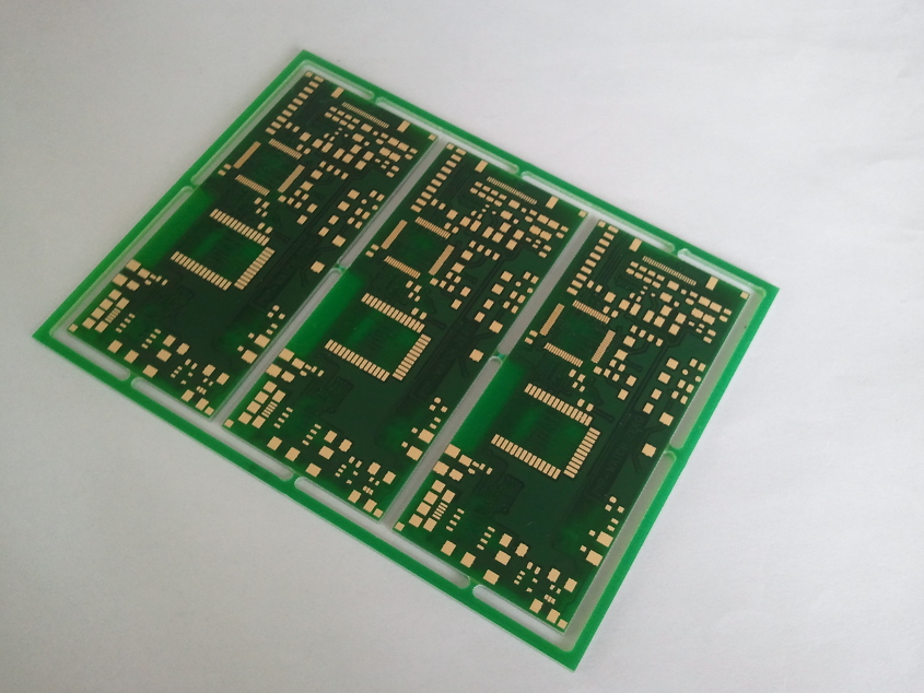 PIP-Watch Zero: Pristine PCBs from fab[/caption]
On Saturday I assembled one board, and on Sunday I tested it and started working on firmware. I had some problems with PLL in the microcontroller - the CPU hard-resetted the instant the PLL was enabled. Eventually I found a bad solder joint on one of the CPU’s power supply pins.
Posts
read more
PIP-Watch "Zero" - Schematic, BOM, and Layout
Schematic [PDF], BOM, and PCB layout for my PIP-Watch “Zero” was completed during this week. Layout data was sent to a local PCB fab - pragoboard.cz. The board should be ready and shipped during the next week.
The PCB is is 80mm*35mm. The top side is dedicated to the EPD display, battery (underneath the display), 3 push-buttons and 4 LEDs. The bottom side carries all the main electronics - processor, bluetooth modem, display driver, and power source.
Posts
read more
FreeRTOS tasks and queues
In my previous homebrew projects I did not use any operating system in the embedded processors. Software was programmed on a bare-metal hardware. In my Talking Clock project I created a simple cooperative event-processing abstraction layer, but it was very limited.
Posts
read more
Framebuffer Drawing with u8glib [VIDEO]
GDE021A1 is a graphics display with a resolution 172x72 pixels, each pixel is 2 bits deep (4 shades of grey). The display has an internal controller SSD1606 with a framebuffer. The framebuffer size is 172*72*2/8=3096 Bytes. When the display is powered up, the system processor sends initialization sequence that first sets up controller’s internal registers (the controller SSD1606 is fairly generic) and then sends new framebuffer content. The display controller then autonomously pushes the framebuffer contents to the physical screen.
The display controller can be configured to orient the framebuffer almost any way. I configured it into a landscape mode, with the X-axis going right and the Y-axis down, as shown on the photo.
Posts
read more
EPD Display Working!
Today I have managed to get the GDE021A1 ePaper display (EPD) working! I used my minimal EPD-Driver board, which implements a flat-flex cable connector and a booster circuit for the display. The booster generates high voltages needed for display operation (around +-25V). The display is driven by STM32F101 Cortex-M3 CPU, mounted on a universal PCB. The picture below depicts my workbench setup (click to see a full-size image):
[caption id=“attachment_410” align=“aligncenter” width=“1205”] EPD Driver Prototype-workbench view with captions[/caption]
Posts
read more
Li-On Battery Charging (and Discharging)
In my PIP-Watch project I will use a Li-On battery to provide power. Li-On batteries are easy to use in hobby projects: they are light, small, with high capacity, and they come in variety of sizes. Most (not all) Li-On batteries have nominal voltage 3.7V, hence you can directly power your standard 3.3V digital logic directly, using only a simple low-drop linear regulator (e.g. LD59015).
For my first experiments I chose Nokia BL-4C Li-On battery. It’s nominal voltage is 3.7V, charging (maximal) voltage is 4.2V, the capacity is 860mAh.
Posts
read more
Bluetoothing to Android Tablet
Today I tried pairing my UART-to-Bluetooth adapter to a Nexus 7 tablet to see how it works. On the tablet I used BlueTerm, an open-source terminal emulator for communicating with any serial device using a bluetooth serial adapter.
I connected my Bluetooth adapter through a USB/UART adapter to a PC. On the PC in a terminal emulator the following sequence of commands is sent to the BT adapter:
///
at*agln="PIP-Watch",0
at*agfp="1234",0
at*addm
The three slashes are an escape sequence to put the adapter into the AT-mode. Then we set BT device name and a PIN. Finally we exit the AT-mode, entering data mode. The adapter now awaits BT connections.
Posts
read more
Foolish Attempt at Soldering an FPC Connector with 0.5mm Pitch, and a Prototyping PCB Design
Mechanical drawing of my EPD ePaper display GDE021A1 is shown below. Signals to the display are connected via a 24-pin flex flat cable. The pitch between pins is only 0.5mm. A suitable matching connector is MOLEX 52435-2471 FPC RCPT 24PIN 1ROW.
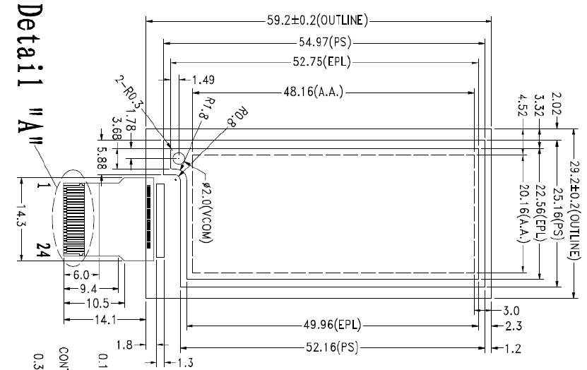
On Thursday I tried soldering thin wires directly on the MOLEX connector I got from Farnell. However, my attempt was very naïve because the pitch between pins on the connector is only 0.5mm. So I failed.
Posts
read more
New Project: PIP-Watch
I started a new project called PIP-Watch: Personal Information Panel/Watch. It will be a kind of smartwatch. It will use an ePaper display and a bluetooth connection to a smart-phone.
I also registered the project on hackaday.io, to take part in this year’s Hackaday Prize, which will send one hacker into space!
Posts
read more
Bluetooth Module (Re-)Investigation
Some five years ago I bought a nice UART-over-Bluetooth adapter module. The module emulates a serial port (UART) over a Bluetooth connection. All necessary chips and an antenna are mounted on a small PCB board depicted below.
The type I’ve got is the cB-OEMSPA310i-04 with an internal antenna. The module requires only a 3.3V power.
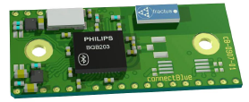
Communication with the module is over serial UART at 3.3V logic levels. The basic RXD/TXD signal pair is complemented with hardware flow control via RTS/CTS, and an optional BT connection status via DSR/DTR. A three-colour LED (red, blue, green) can be directly connected to dedicated pins on the module to visually indicate the state of module to the user.
The BT module is controlled by standard AT commands. When powered up or after a reset the module is in a data mode with no connection over BT. Local application microcontroller connected to the RXD/TXD/RTS/CTS signals first sends an escape sequence, which normally consists of three forward slashes ‘///’. This puts the module into the AT mode. In AT mode the strings sent over the local UART are interpreted as commands, while in data mode all data is passed through to bluetooth and over the air.
Category: Hackaday_2014
Posts
read more
Bluetooth Power Modes
In previous post we discussed CPU power consumption in PIP-Watch. Today we look into Bluetooth power consumption because it is significant as much as the CPU power.
Posts
read more
Processor Low-power Optimizations in PIP-Watch
Processor Power
The PIP-Watch is a battery-powered device that will be continuously on, hence the average power consumption is one of the most important engineering aspects.
In this post I will go through two simple steps of optimizing CPU power - sleep modes and lowering the clock frequency. In a next separate post we will look into Bluetooth module power.
Posts
read more
PIP-Watch Boards & Assembly
The printed circuit boards for PIP-Watch Zero came from Pragoboard fab on Friday 12 Sept. I ordered three pieces because the cost is practically identical as for two or one.
[caption id=“attachment_484” align=“aligncenter” width=“845”] PIP-Watch Zero: Pristine PCBs from fab[/caption]
On Saturday I assembled one board, and on Sunday I tested it and started working on firmware. I had some problems with PLL in the microcontroller - the CPU hard-resetted the instant the PLL was enabled. Eventually I found a bad solder joint on one of the CPU’s power supply pins.
Posts
read more
PIP-Watch "Zero" - Schematic, BOM, and Layout
Schematic [PDF], BOM, and PCB layout for my PIP-Watch “Zero” was completed during this week. Layout data was sent to a local PCB fab - pragoboard.cz. The board should be ready and shipped during the next week.
The PCB is is 80mm*35mm. The top side is dedicated to the EPD display, battery (underneath the display), 3 push-buttons and 4 LEDs. The bottom side carries all the main electronics - processor, bluetooth modem, display driver, and power source.
Posts
read more
FreeRTOS tasks and queues
In my previous homebrew projects I did not use any operating system in the embedded processors. Software was programmed on a bare-metal hardware. In my Talking Clock project I created a simple cooperative event-processing abstraction layer, but it was very limited.
Posts
read more
Framebuffer Drawing with u8glib [VIDEO]
GDE021A1 is a graphics display with a resolution 172x72 pixels, each pixel is 2 bits deep (4 shades of grey). The display has an internal controller SSD1606 with a framebuffer. The framebuffer size is 172*72*2/8=3096 Bytes. When the display is powered up, the system processor sends initialization sequence that first sets up controller’s internal registers (the controller SSD1606 is fairly generic) and then sends new framebuffer content. The display controller then autonomously pushes the framebuffer contents to the physical screen.
The display controller can be configured to orient the framebuffer almost any way. I configured it into a landscape mode, with the X-axis going right and the Y-axis down, as shown on the photo.
Posts
read more
EPD Display Working!
Today I have managed to get the GDE021A1 ePaper display (EPD) working! I used my minimal EPD-Driver board, which implements a flat-flex cable connector and a booster circuit for the display. The booster generates high voltages needed for display operation (around +-25V). The display is driven by STM32F101 Cortex-M3 CPU, mounted on a universal PCB. The picture below depicts my workbench setup (click to see a full-size image):
[caption id=“attachment_410” align=“aligncenter” width=“1205”] EPD Driver Prototype-workbench view with captions[/caption]
Posts
read more
Li-On Battery Charging (and Discharging)
In my PIP-Watch project I will use a Li-On battery to provide power. Li-On batteries are easy to use in hobby projects: they are light, small, with high capacity, and they come in variety of sizes. Most (not all) Li-On batteries have nominal voltage 3.7V, hence you can directly power your standard 3.3V digital logic directly, using only a simple low-drop linear regulator (e.g. LD59015).
For my first experiments I chose Nokia BL-4C Li-On battery. It’s nominal voltage is 3.7V, charging (maximal) voltage is 4.2V, the capacity is 860mAh.
Posts
read more
Bluetoothing to Android Tablet
Today I tried pairing my UART-to-Bluetooth adapter to a Nexus 7 tablet to see how it works. On the tablet I used BlueTerm, an open-source terminal emulator for communicating with any serial device using a bluetooth serial adapter.
I connected my Bluetooth adapter through a USB/UART adapter to a PC. On the PC in a terminal emulator the following sequence of commands is sent to the BT adapter:
///
at*agln="PIP-Watch",0
at*agfp="1234",0
at*addm
The three slashes are an escape sequence to put the adapter into the AT-mode. Then we set BT device name and a PIN. Finally we exit the AT-mode, entering data mode. The adapter now awaits BT connections.
Posts
read more
Foolish Attempt at Soldering an FPC Connector with 0.5mm Pitch, and a Prototyping PCB Design
Mechanical drawing of my EPD ePaper display GDE021A1 is shown below. Signals to the display are connected via a 24-pin flex flat cable. The pitch between pins is only 0.5mm. A suitable matching connector is MOLEX 52435-2471 FPC RCPT 24PIN 1ROW.
On Thursday I tried soldering thin wires directly on the MOLEX connector I got from Farnell. However, my attempt was very naïve because the pitch between pins on the connector is only 0.5mm. So I failed.
Posts
read more
New Project: PIP-Watch
I started a new project called PIP-Watch: Personal Information Panel/Watch. It will be a kind of smartwatch. It will use an ePaper display and a bluetooth connection to a smart-phone.
I also registered the project on hackaday.io, to take part in this year’s Hackaday Prize, which will send one hacker into space!
Posts
read more
Bluetooth Module (Re-)Investigation
Some five years ago I bought a nice UART-over-Bluetooth adapter module. The module emulates a serial port (UART) over a Bluetooth connection. All necessary chips and an antenna are mounted on a small PCB board depicted below.
The type I’ve got is the cB-OEMSPA310i-04 with an internal antenna. The module requires only a 3.3V power.
Communication with the module is over serial UART at 3.3V logic levels. The basic RXD/TXD signal pair is complemented with hardware flow control via RTS/CTS, and an optional BT connection status via DSR/DTR. A three-colour LED (red, blue, green) can be directly connected to dedicated pins on the module to visually indicate the state of module to the user.
The BT module is controlled by standard AT commands. When powered up or after a reset the module is in a data mode with no connection over BT. Local application microcontroller connected to the RXD/TXD/RTS/CTS signals first sends an escape sequence, which normally consists of three forward slashes ‘///’. This puts the module into the AT mode. In AT mode the strings sent over the local UART are interpreted as commands, while in data mode all data is passed through to bluetooth and over the air.
Category: Tools
Posts
read more
Voltcraft VC-870 Multimeter Used With UNI-T UT-D04 USB Cable
Target hardware:
Software repository location:
The issue this software solves: Although the Voltcraft multimeter and the UNI-T USB cable are hardware compatible (the USB cable adapter fits into the multimeter connector perfectly), the software requirements are different. Original Voltcraft USB cable, which costs tripple the UNI-T cable by the way, mimics RS232 adapter when plugged in USB host PC. The UNI-T cable uses different chip internally and behaves like a HID device. On the other hand, UNI-T multimeters use different communication protocol over the serial line than the VC870 does.
Posts
read more
Philips PM3310 Digital Storage Oscilloscope
I got myself an old Philips PM3310 Digital Storage Oscilloscope (DSO). The scope has a classic CRT screen, but otherwise it is a fully digital device. The scope has two channels. Analogue bandwidth of the input attenuator/amplifier is 60MHz, which is not bad at all. Sampling frequency in real-time mode, however, is only 50 Mega samples per second. Each sampling ‘run’ after a trigger stores 256 samples into a RAM. The sample RAM has capacity for 4 independent waveforms. The 50M sampling speed allows single-shot time base up to 500ns/div, and a recurrent time base up to 5ns/div (sampling of repetitive signals in equivalent time). The internal CPU switches between the modes as needed.
Posts
read more
Xilinx Vivado 2013.3 on Fedora 18: Working around a D-Bus bug
Running Xilinx Vivado 2013.3 (webpack license) on Fedora 18 may fail with the following error message:
$ vivado

****** Vivado v2013.3 (64-bit)
  **** SW Build 329390 on Wed Oct 16 18:26:55 MDT 2013
  **** IP Build 192953 on Wed Oct 16 08:44:02 MDT 2013
    ** Copyright 1986-1999, 2001-2013 Xilinx, Inc. All Rights Reserved.

INFO: [Common 17-78] Attempting to get a license: Implementation
process 17688: arguments to dbus_move_error() were incorrect, assertion "(dest) == NULL || !dbus_error_is_set ((dest))" failed in file dbus-errors.c line 282.
This is normally a bug in some application using the D-Bus library.
  D-Bus not built with -rdynamic so unable to print a backtrace
Abnormal program termination (6)
Please check '/home/jara/hdl/hs_err_pid17688.log' for details
The workaround is to make the D-Bus communication socket file /var/run/dbus/system_bus_socket unavailable when the Xilinx tools run.
Category: Nixietech
Posts
read more
Talking Clock: COMPLETED!
Finally I declare the Talking Clock project complete! Hardware is built and is working, documentation has been written.
The permanent project web page is here. I have also created a parallel page on hackaday.io. Enjoy!
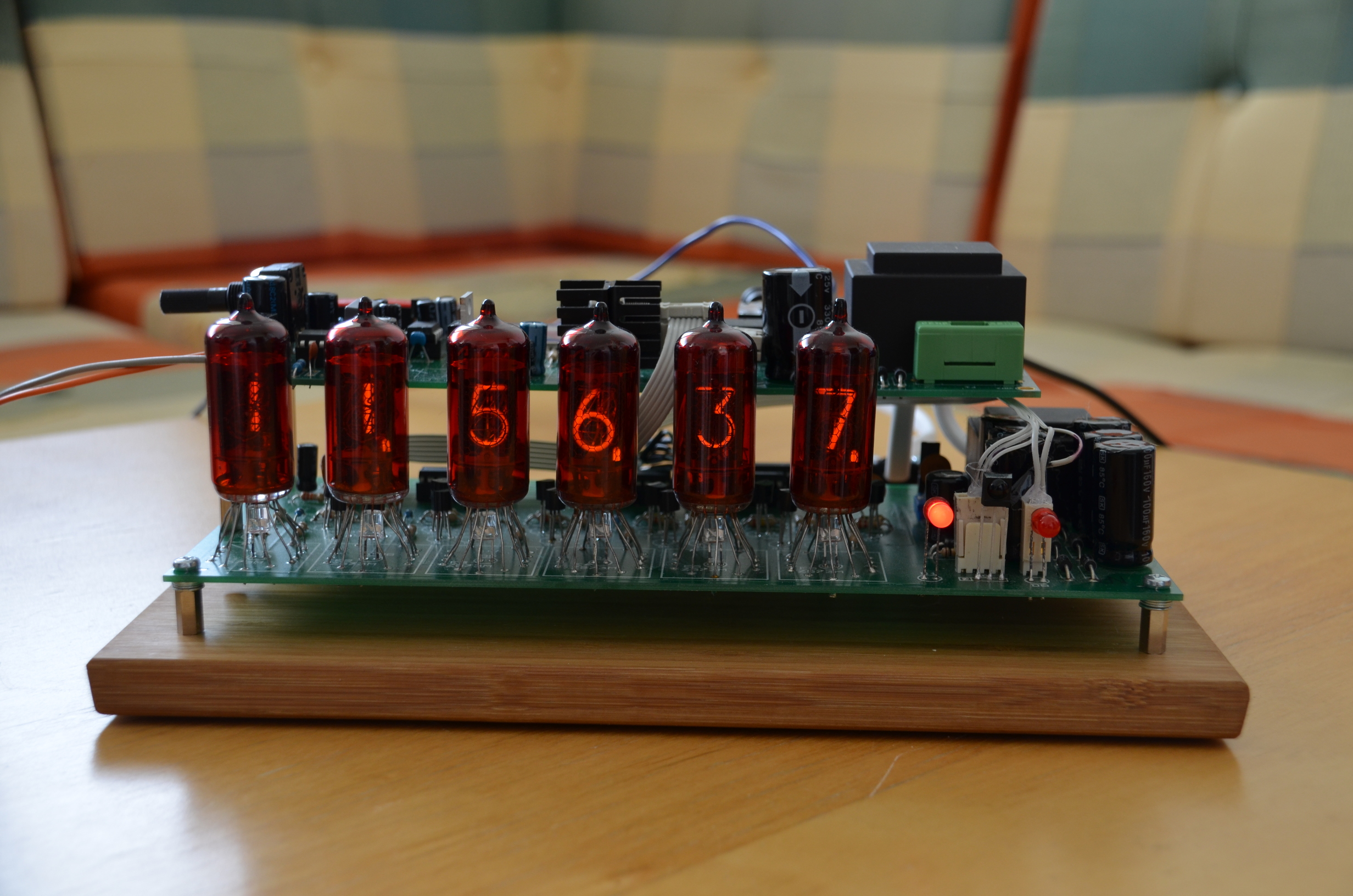
Posts
read more
Talking Nixie Clock
I’ve just assembled both PCB boards of my talking nixie clock together and went ‘whoa, this thing IS really beautiful!’. Check it out below, electronics porn at its best!
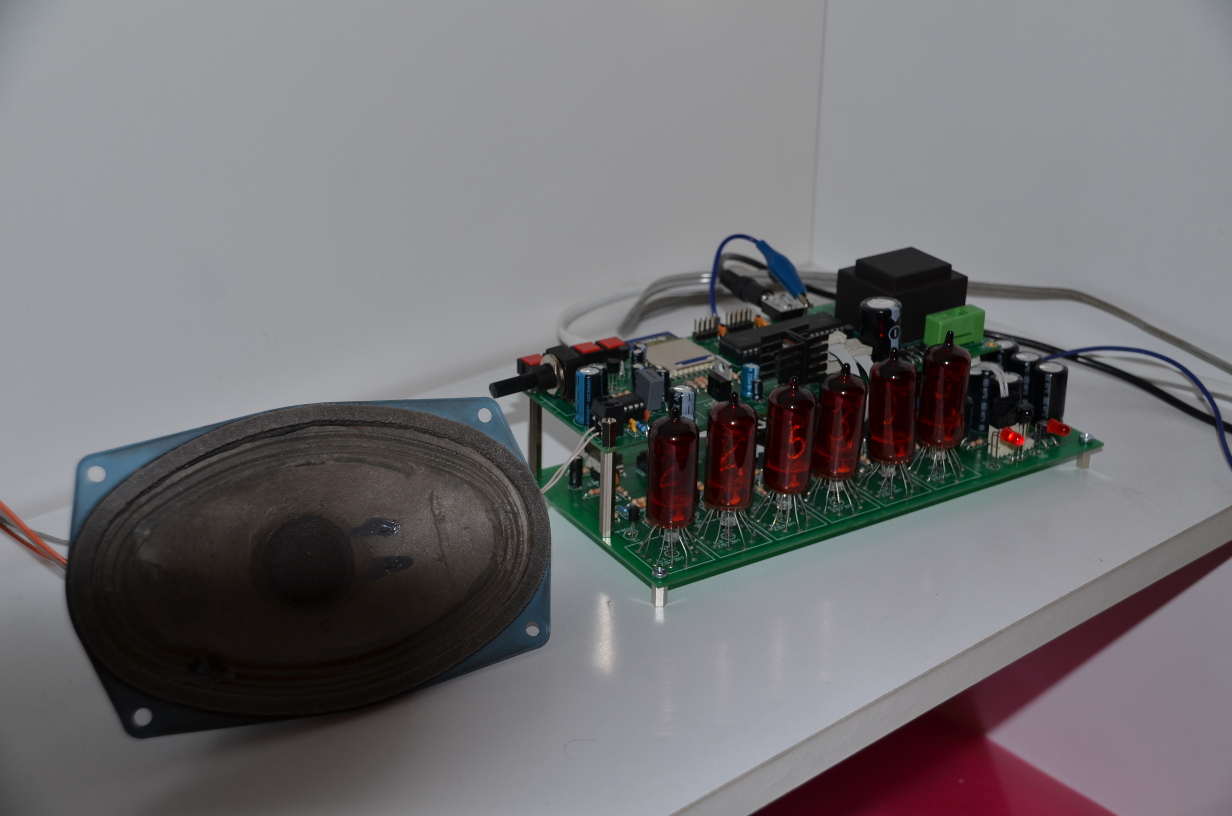
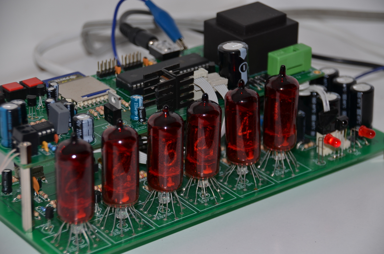

The first two pictures were taken with a flash to get good details, the last one without, hence a poorer picture quality. But you at least get the idea how those nixie puppies shine!
Later I’ll get my documentation together and create a proper project page with all schematics, pcbs, source codes, better pictures etc etc.
Posts
read more
Talking Clock Prototype
I am working on a talking clock with a remote IR control. The idea is that when I awake at night I don’t have my glasses on, hence I cannot recognize digits on a clock display. So I figured out that what I need is a talking clock that could tell me the time aloud. The audible announcement is triggered by a button press on a standard infrared remote, normally used to control my hi-fi equipment.
Category: Talking-Clock
Posts
read more
Talking Nixie Clock
I’ve just assembled both PCB boards of my talking nixie clock together and went ‘whoa, this thing IS really beautiful!’. Check it out below, electronics porn at its best!
The first two pictures were taken with a flash to get good details, the last one without, hence a poorer picture quality. But you at least get the idea how those nixie puppies shine!
Later I’ll get my documentation together and create a proper project page with all schematics, pcbs, source codes, better pictures etc etc.
Posts
read more
Talking Clock Prototype
I am working on a talking clock with a remote IR control. The idea is that when I awake at night I don’t have my glasses on, hence I cannot recognize digits on a clock display. So I figured out that what I need is a talking clock that could tell me the time aloud. The audible announcement is triggered by a button press on a standard infrared remote, normally used to control my hi-fi equipment.