Powering the Agilex 3 FPGA
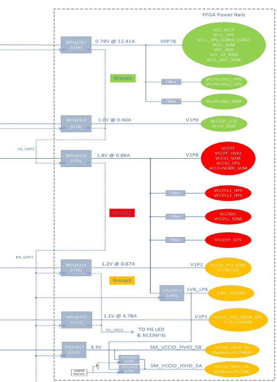
The picture below is an extract from Power-Supply Block Diagram of the official Agilex 3 Devkit. The FPGA requires multiple power supply levels: from 0.75V to 3.3V. Specification is found in altera document Power Management User Guide: Agilex™ 3 FPGAs and SoCs and details for particular device in Agilex™ 3 FPGAs and SoCs Device Data Sheet.
Minimum Set of Power Levels
This is the list of mandatory power supply levels needed for the Agilex 3 FPGA:
-
0.75V - for the core (valid for the slower -7S version; for the faster -6S the core voltage should be increased to 0.78V)
-
1.20V - for the core and SDM
-
1.80V - for basic I/O including SDM
Configuration of some power rails of the FPGA depends on user design. These are typically:
-
1.10V - for LP4 EMIF
-
3.30V - for other legacy GPIO, as needed.
Power Sequencing
Power voltage supply pins are assigned in 3 groups, named “1”, “2A” and “2B” in the Altera guide. (The devkit blockdiagram reproduced above uses just different naming 1, 2, and 3.) The groups must be brought up one after another in a sequence. The table below assigns the FPGA pins to rails split in the groups:
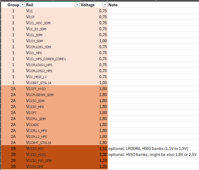
Thankfully each voltage level is only in one group:
-
Group 1:
-
0.75V (valid for the -7S (slower) device; for faster -6S it should be increased to 0.78V)
-
1.00V
-
-
Group 2A:
- 1.80V
-
Group 2B:
-
1.10V (optional - HSIO, LP4)
-
1.20V
-
3.30V (optional - HVIO)
-
System Considerations
In supply sequencing it is necessary to consider the requirements of all devices on the board together. In case of the Devkit board the additional critical component is the LPDDR4 memory device.
The following table is from Micron MT53E512M32D1, MT53E1G32D2 datasheet:
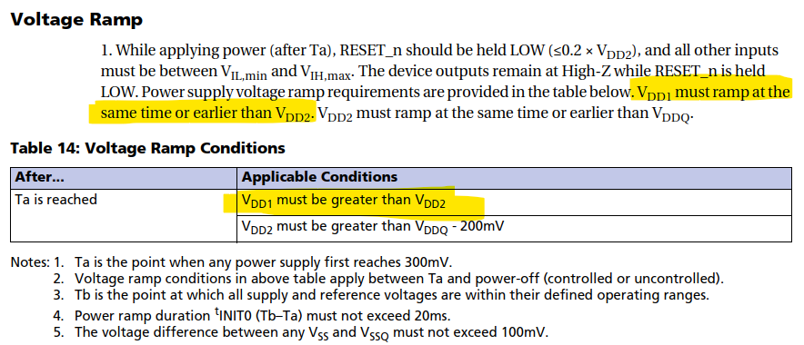
In LPDDR4, VDD1=1.8V and VDD2=VDDQ=1.1V, nominal. Therefore, it is necessary to ramp up the 1.8V first and then 1.1V, OR both together. This LPDDR4 requirement is conformant to the FPGA requirements, which places the 1.8V source in group 2A and the 1.1V source in group 2B.
In case of the Agilex 3 Devkit, they rather choose to ramp both supplies of LPDDR4 together, by implementing an additional load switch TPS22917 (U46) - highlighted in yellow below:
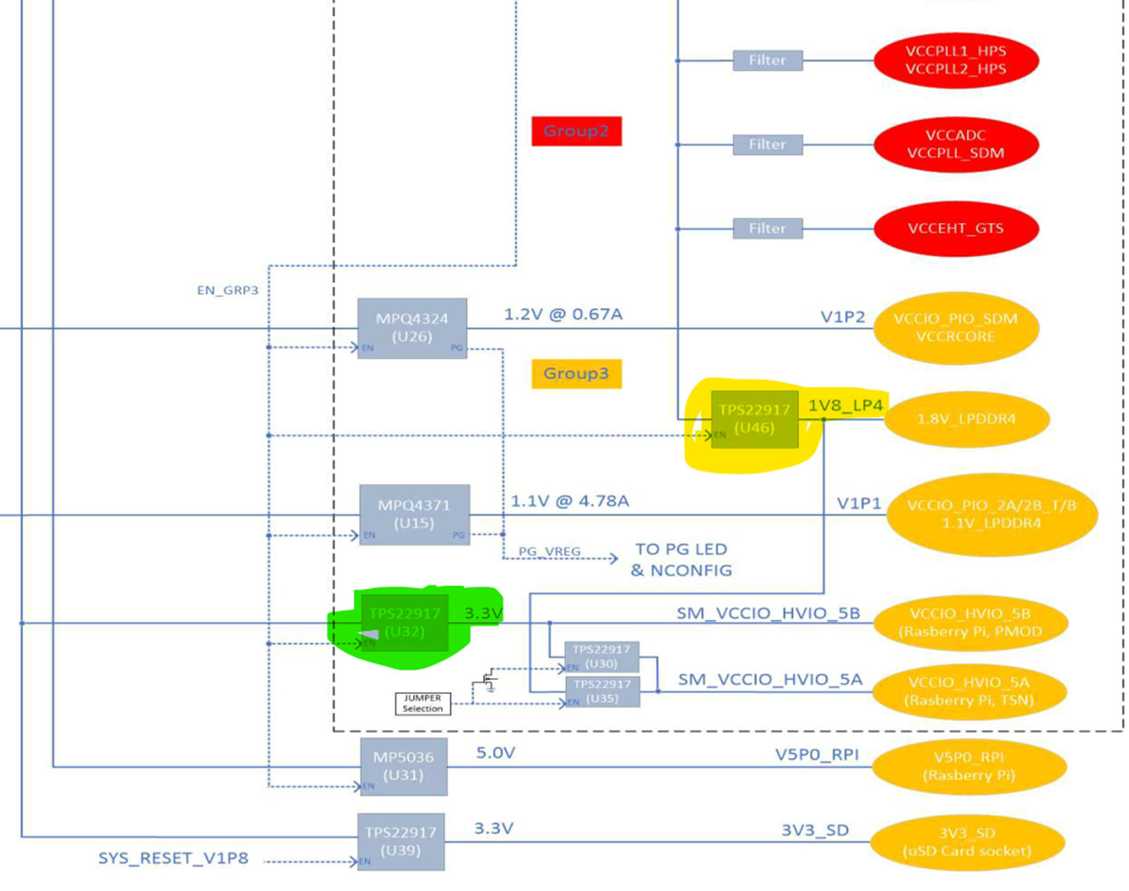
The switch U46 for 1.8V_LPDDR4 is enabled together with the DC/DC converter for 1.1V (signal EN_GRP3).
There is another load switch U32, marked green above, which enables the 3.3V to the FPGA, which is necessary to do last (FPGA group 2B).
Power Consumption Estimation
Supply currents shown in the Devkit PSU block diagram above are wildly overestimated. The reason is that the same board also supports more powerful pin-compatible Agilex 5 devices, including the full HPS subsystem and bigger array size.
As already discussed in a previous post, one has to use Altera’s Power and Therman Analyzer to get the estimate of the FPGA power consumption.