This is Part 1 of the two-part series on Ethernet RMII. Part 2 is also available.
Imagine your application requires a non-standard periphery controlled by an embedded processor. What options do you have? The periphery can be implemented in an FPGA; depending on periphery complexity you can choose an optimal FPGA that fits your budget. Where the processor goes? There are three possibilities: (a) inside FPGA as a soft-core → it will increase the cost of FPGA (larger type needed) and complicate HDL and software design. Or (b) inside FPGA as a hard-core → a nice compact solution and quite possible with heterogeneous FPGA from Xilinx (Zynq) and Altera (SoC). But the cost of these modern devices could still be too high for price sensitive applications. You must fit both your software and HDL to pre-engineered combinations of FPGA and ARM CPU sizes (perhaps a small Cortex-M core would suffice but you must pay for a gigahertz-class Cortex A cores).
The third option (c) is using a stand-alone MCU (maybe even not an ARM) and a standard FPGA. How do you connect them? You are limited to interfaces offered by the MCU. In modern low-end MCUs (by that I mean smaller STM32Fxxx devices) you have I2C (400 kbit/s), UART (115 kbit/s), SPI (~10Mbit/s), Fast Ethernet (100 Mbit/s). So what about the Ethernet core in the MCU? Could it be used to interface with FPGA? Sure it can!
Hardware Configuration
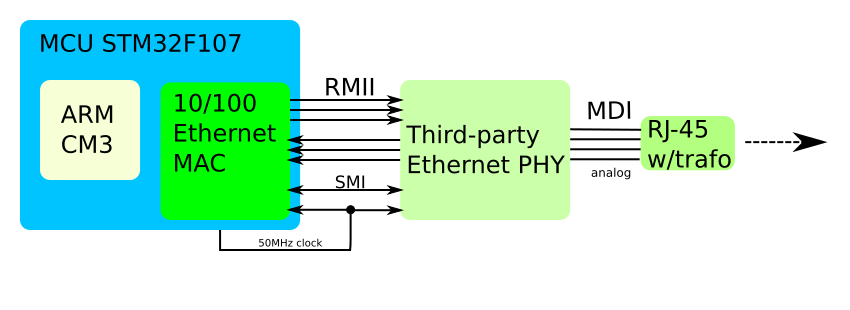
Here is my test setup. I am using STM32F107 MCU that has an integrated 10/100Mbit Ethernet core but without an integrated PHY. The Ethernet core (MAC) normally interfaces with an external PHY via a digital MII or RMII interface. Both interface types – MII and RMII – have nominal bandwidth 100Mbit/s (in Fast Ethernet), but RMII has the advantage of using fewer signals: MII requires 14 wires operating at 25MHz, while RMII requires 6 wires operating at 50MHz. So I will use RMII.
On the FPGA side I am using the ZED Board with Zynq XC7Z020 FPGA. It is surely an overkill in this demo but it allows for fast prototyping. Zynq includes dual-core ARM processors.
Basic Frame Sending
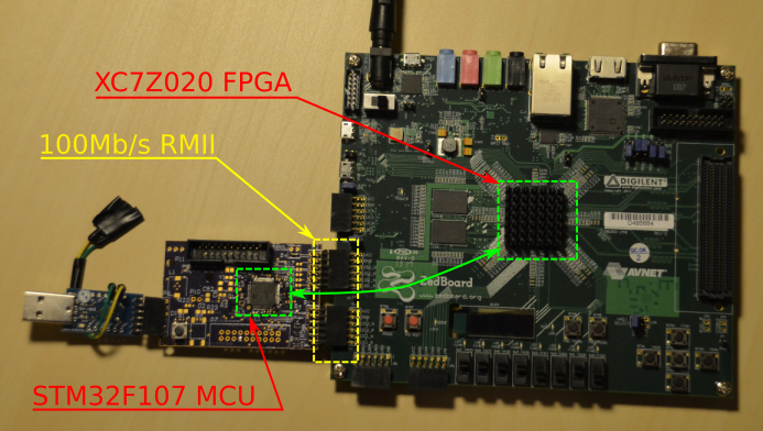
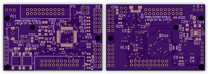
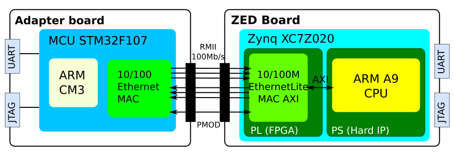
The first experiment demonstrates physical hardware interconnection. MCU STM32F107 in LQFP64 package is mounted on a special adapter PCB that I designed in Circuit Maker (I find it good, but not excellent and I will probably revert back to KiCAD.). Schematic design [pdf] of this PCB includes many other components, but for this test we really need to assemble just the MCU, JTAG connector 2x10p, UART connector, and two PMOD pin-headers 2x6p connectors. The board connects to ZED board via two PMOD connectors – on ZED it is JC1 and JD1. Only JC1 signals are actually used in this demo. Power 3.3V is drawn directly from ZED.
This is signal routing from the STM MCU via connectors to the FPGA:
| RMII Signal | STM Sig/Pin | Dir. | ZED PMOD JC1 pin nr. | ZED Signal | Zynq Ball |
| TXEN | PB11 / p30 | -> | 4 | JC2_N | AA4 |
| TXD0 | PB12/ p33 | -> | 8 | JC3_N | T6 |
| TXD1 | PB13 / p34 | -> | 7 | JC3_P | R6 |
| CRSDV | PA7 / p23 | <- | 3 | JC2_P | Y4 |
| RXD0 | PC4 / p24 | ← | 2 | JC1_N | AB6 |
| RXD1 | PC5 / p25 | ← | 1 | JC1_P | AB7 |
| REFCLK_O | PA8 / p41 | <- | 9 | JC4_P | T4 |
(Note: PMOD connector is a standard pin-header/socket with 2.54mm pitch, but they use non-standard pin numbering in ZED schematic.)
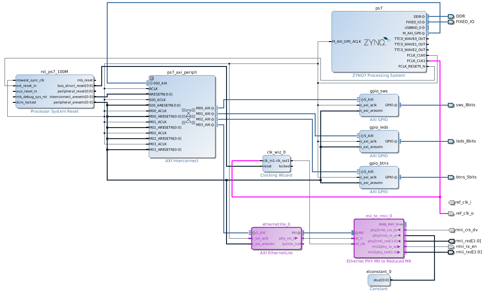
Figure below shows the internal design in Zynq FPGA. It uses only standard Xilinx IP core components available with free Web-pack license in Vivado 2015.03. RMII input/output signals are connected to the MII/RMII converter named ‘mii_to_rmii_0’. Signals are converted to MII standard and routed to AXI Ethernet Lite core named ‘ethernetlite_0’. This simple core allows TX/RX of frames at 10/100Mbps speeds. It is entirely controlled by software running in Zynq ARM core. Software in Zynq ARM must configure the core and continuously transfer data directly to/from its internal block-RAMs (there is no DMA with this core).
There are two software loads in this demo: in STM32F107 and in Zynq. In both firmwares I use FreeRTOS operating system. Not because it is required, but it makes some things easier if you know what you are doing. In STM32 there is a standard peripheral library that also includes basic Ethernet driver which can send and receive raw frames. In Zynq there are Xilinx IP drivers; the driver for AXI Ethernet Lite core can send and receive raw frames. My programs allow to send a frame upon a button press and dump received frames to UART for inspection – symmetrically on both ends.
Structure of Ethernet Frames
Ethernet frames have a pre-defined structure that is wise to follow even in this non-standard application. Each frame is up to 1500 octets (bytes) long. The first eight bytes are always constant; they serve to synchronize bit clocks in distant receivers with that in a transmitter. The constant value is 10101010 10101010 10101010 10101010 10101010 10101010 10101010 10101011, transmitted left to right. In hexadecimal it is 0x55 0x55 0x55 0x55 0x55 0x55 0x55 0xD5, with LSB first. These bytes are called preamble bytes (0x55…) and the start-frame-delimiter or SFD byte (it is the last byte with value 0xD5).
Directly after the SFD byte there are 6 bytes of destination MAC address and then 6 bytes of source MAC address. Destination MAC address is filtered in receivers (if it is not in promiscuous mode) so it is good idea to have it set to some sensible value. After these 12B of MAC addresses there are 2 bytes of EtherType/Length field. This field is treated as one 16-bit value (the higher-ordered byte is transmitted first). For historical reasons this field can contain either frame length in bytes (a value <= 1500), or protocol type ID of payload. Type IDs are constants assigned by standard. For example, 0x0800 identifies IPv4, 0x0806 is ARP, and so on. As all type IDs are values grater than 1536 decimal there is no confusion if the field is used for length or type. Presently the type interpretation is preferred.
After the EtherType/Length field the data payload starts. Minimum payload size is 46B. It extends just 4B before the end of frame. Before the end of frame there are 4B of frame checksum sequence (FCS), which is 32-bit CRC. The FCS/CRC code is computed over the whole frame starting at the first Destination MAC byte and ending with the last payload byte (preamble and SFD are excluded). The CRC32 code used in Ethernet and other IEEE 802 protocols has a useful property that if receivers calculate the code over the whole frame including the received FCS/CRC field, it must obtain a constant residue 0xC704DD7B.
The standard prescribes a minimum inter-frame gap between successive frames. In 100Mbit Ethernet it is 96-bits, i.e. 12B or 0.96us. MAC transceiver in STM32 allows to configure a smaller gap (40b) to better utilize channel, if needed.
In part 2 I will describe my own implementation of a simple MAC core in FPGA suitable for direct MCU-FPGA usecase, and there will be more experiments!
Source code is available on github in project jsyk/miilink.


Hi,
Thanks for the great post. Which software are you using for block diagrams ?
It’s the open-source Inkscape.
Thanks buddy.
how to convert mii data into rmii and vice-versa