This is Part 2 of a two-part series on Ethernet RMII. In Part 1 I described my hardware setup and basic Ethernet operation. In the second and final part I will describe the design of specialized MAC cores I implemented on FPGA, and there will be measurements to see how much throughput and latency the system can achieve.
Real Throughput of Fast Ethernet
Lets calculate the throughput and latency of a 100Mbps Fast Ethernet connection. One bit interval is 10ns long. Each frame accounts the following fields: preamble with SFD (7B+1B), destination MAC (6B), source MAC (6B), type (2B), payload (variable, minimum 46B), FCS/CRC (4B), inter-frame gap (12B). The sum of length of all fixed fields is 7+1+6+6+2+4+12 = 38B, or 304b, or 3.040us. Payload must be padded if less than 46B of user data are to be transmitted. The minimum frame length including inter-frame gap is 84B, which corresponds to 6.7us of channel time.
Graph below plots real throughput in kB/s relative to the amount of user data transmitted in one frame (blue line). Horizontal axis is logarithmic. For instance, if only 1B of user data must be transmitted, due to protocol restrictions the payload field must be padded by 45B and the frame will be 84B long (inc. gap). If only 1B-user-data frames are transmitted over the line the real throughput will be only 145kB/s ! The graph compares also with SPI running at 18MHz clock speed (maximum for STM32F107) and an SPI running at 48MHz (1b data width). The former has a constant throughput 2197kB/s, the later 5859kB/s. Compared to SPI @ 18MHz Ethernet is faster starting at 16B of user data per frame (2325kB/s). It is faster than SPI @ 48MHz starting at 46B of user data per frame.
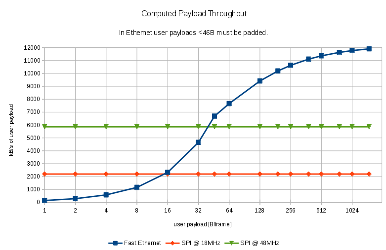
Computed Payload Throughput
Frame Transport over RMII
On hardware level frames are transmitted over RMII from MAC to PHY. The PHY encodes frame data to analogue signals for transmission over twisted pair copper wires. I will not discuss PHY operation here further.
Complete frames including preamble and SFD bytes are transported over RMII with LSB first. RMII sends two bits of data on each clock rising edge, hence one byte is transmitted in 4 clock pulses over the RMII_TXD[0] and RMII_TXD[1] signals. The signal RMII_TXEN is kept high for the whole duration of frame transmission.
In the other direction the frame transport proceeds the same way. Complete frame is received on RMII_RXD[0] and RMII_RXD[1] lines, LSB first, 2 bits at a time. Sadly, in RMII the RXCRSDV signal is not perfect mirror of the TXEN signal as two data values are multiplexed in this signal on alternate clock edges: the data-valid RX_DV (which is a true mirror of TXEN) and a carrier sense (CRS). However, in our application without a PHY we can ignore the CRS functionality and just assume that signal RMII_RXCRSDV is a mirror of TXEN. Of course signal connections between STM32 and Ethernet Lite in Zynq must be crossed (STM32 TX→ Ethernet Lite RX).
Specialized Ethernet MAC
Standard Ethernet MAC cores must be controlled and supported from an embedded CPU in the FPGA. They are not meant for stand-alone operation. Hence I have designed my own MAC core specifically for the application discussed here. My MAC core is stripped down in functionality. It supports only 100Mbps Ethernet over RMII, full-duplex. There is no SMI interface because there is no PHY.
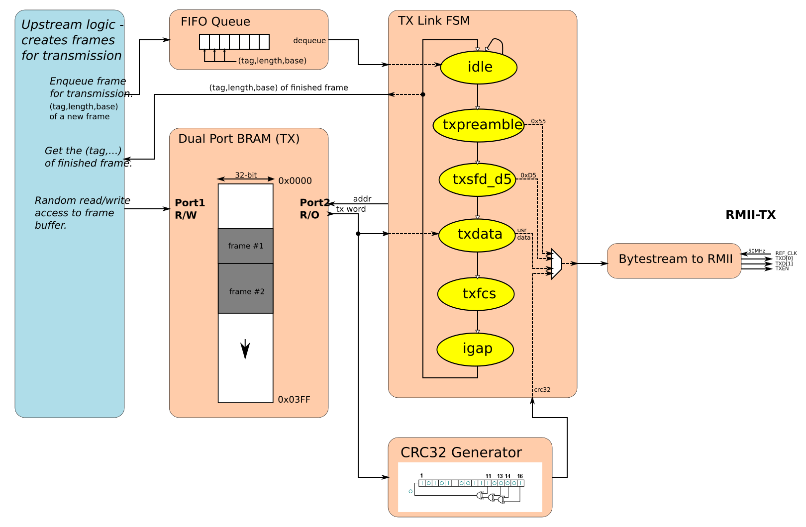
Special TX-MAC for FPGA
Figure above shows block structure of transmit path (MAC TX). On the left there is upstream logic that creates new Ethernet frames for transmission. It writes raw frames to the dual-ported Block-RAM depicted in the middle. The BRAM is organised in 32-bit words and a configurable address width (depicted a 1024-word memory). Raw frames start with a Destination MAC field and end with a payload data; the frame checksum field (FCS) will be calculated and attached automatically. When a new raw frame is ready in the buffer the upstream logic enqueues the tuple (tag, length, base) to the FIFO queue depicted in the mid-top. This tuple is picked up by the transmission automaton (TX Link FSM). The automaton goes through following states: idle (await frame to transmit), txpreamble (send 7*0x55), txsfd_d5 (send 0xD5), txdata (send frame data from the buffer), txfcs (send CRC32), igap (ensure inter-frame gap). CRC32 generator depicted in the mid-bottom calculates the FCS code on-the-fly, then appends it at the end of frame. Serialization of bytes to the 2-bit RMII @ 50MHz happens just at the end of data path.
Special RX-MAC for FPGA
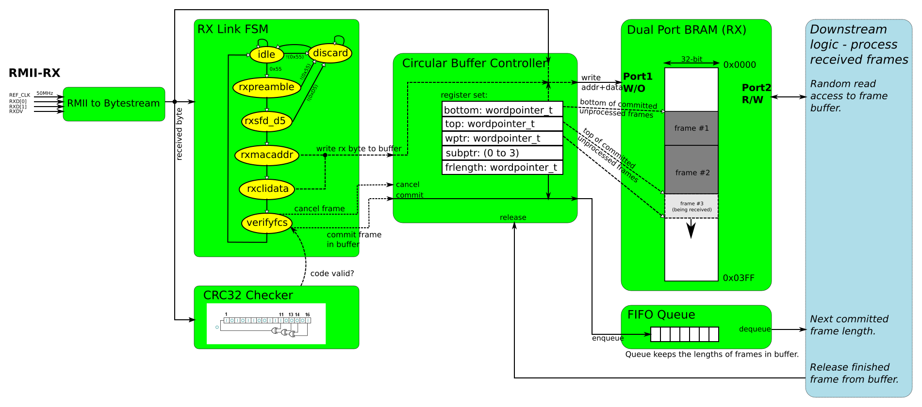
Figure above shows block structure of receive path (MAC RX). At the beginning on the left the 2-bit RMII 50MHz stream is deserialized to bytes. The byte stream is fed in parallel to a reception automaton (RX Link FSM), CRC32 checker and a circular buffer controller. The reception automaton goes through following states: idle (when RXDV is low), rxpreamble (expecting 7*0x55), rxsfd_d5 (expecting the SFD byte 0xD5), rxmacaddr (receiving MAC addresses), rxclidata (receiving rest of frame data), verifyfcs (verifying the CRC code), and discard (ignoring rest of frame in case of errors). Outputs of the automaton control a circular buffer controller depicted in the middle. The circular buffer controller writes received bytes into a dual-ported Block-RAM (a different instance than in the transmission path). In registers the controller keeps bottom and top addresses of used space in the buffer memory, and a current write pointer (wptr). New data is kept in the space between the top and the write pointer; wptr is advanced after each word. Following a successful validation of CRC a new frame is committed in the buffer by moving the top pointer to the write pointer (top := wptr), and simultaneously the frame length is pushed into a FIFO queue. If any error happens during frame reception, CRC validation, or there is insufficient buffer or FIFO space, the frame is dropped by moving write pointer back to the top (wptr := top). Any missing frames must be recognized by downstream logic by way of sequence numbers and trigger retransmission request.
Downstream logic that parses frame payload and acts on it interfaces to the dual-ported BRAM, to the dequeue side of the FIFO queue, and to a release input of the buffer controller. As the frame lengths are pushed into the FIFO queue, the downstream logic knows where each frame begins and ends in the buffer memory by induction from the defined initial condition that the first frame starts at address 0x0000. When the downstream logic is finished with a frame it releases its space in the buffer memory by sending the frame length to the release input of the buffer controller. This increments the bottom pointer by the length (bottom := bottom + length). Frames must be released in the order they are stored in the buffer memory.
Experiments
I evaluated the special Ethernet MAC cores on FPGA with a loopback test setup, of which the block diagram is show below. Zynq FPGA hosts the TX/RX MAC cores and a loop-back core that copies all frames from the receive buffer over to the transmit buffer. Most of received frame data is not modified (it is a loop-back), although the source and destination MAC addresses are exchanged and a couple of data words at the beginning of frame are filled with diagnostic information.
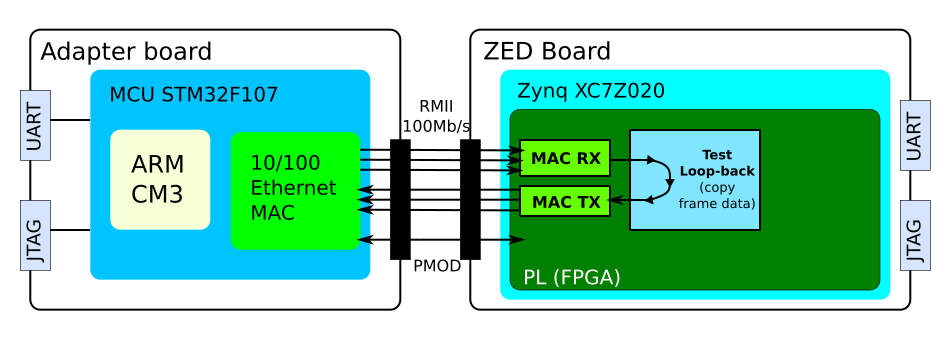
Loopback Demonstrator Block Diagram
FPGA utilization is reported in table screenshot below – see the highlighted lines. The first highlighted line reports on total utilization of the RX, TX and Loopback circuits. Below it the partial utilization of loopback (lb), rx and tx cores is shown. For comparison the last line reports utilization of the Ethernetlite core – a very simple MAC from Xilinx. Clearly there is much space for improvement (e.g. oversized fifo_queue).
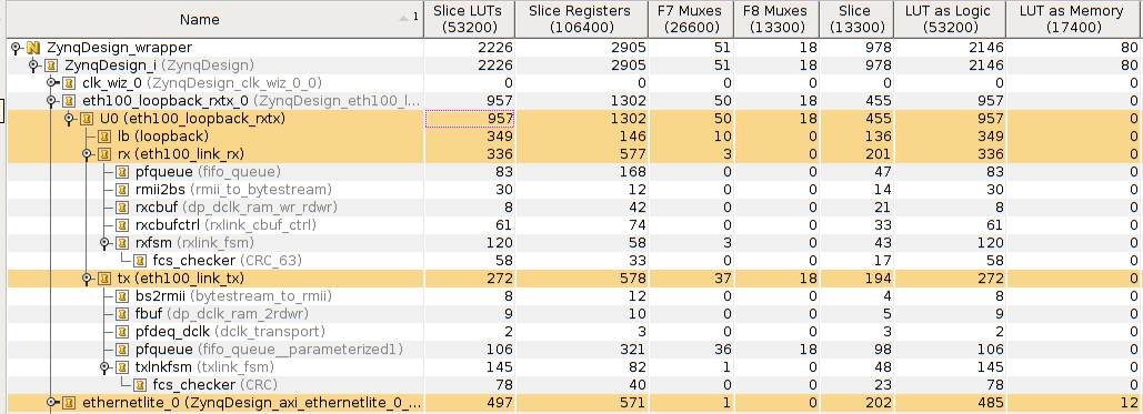
Zynq FPGA Utilization of Resources
Tests are driven by software in STM32 MCU on the adapter board. There is no software needed in Zynq, apart from FPGA bitstream. The STM32 MCU sends frames to the FPGA, which receives them, checks CRC, copies from input buffer to output buffer, then sends again back. The Ethernet MAC core in STM32 MCU has an integrated DMA that transfers data to/from main memory to its hardware send/receive buffers.
Ethernet core in STM32F107 is quite advanced. It has integrated dedicated Ethernet DMA that autonomously transfers frame buffers from main memory to hardware transmit or receive buffers. It can handle many buffers concurrently and offloads much of the work from the CPU. Most importantly, as it is tightly integrated in the MAC core, it can work in cut-through mode. In the normal store-and-forward mode the MAC starts sending a frame out on RMII only when it has been fully transferred into a hardware buffer by TX-DMA; similarly, in the store-and-forward mode RX-DMA begins moving data from an input hardware buffer only after it has been fully received and verified. This method is “safe”, but slow. In cut-through mode the MAC core starts sending data out on RMII immediately after the first 16B has been delivered by TX-DMA; similarly, the RX-DMA starts moving data from hardware buffer to main memory immediately after the first 32B has been received (i.e. long before CRC can be verified). Handshaking between DMA and FIFO queues in MAC is handled fully in hardware.
Pictures below show decomposition of frame round-trip time depending on DMA store-and-forward or cut-through modes. Note that FPGA MAC always operates effectively in a store-and-forward mode because in a real-world use case it would have to do some non-trivial processing on the data, not just forward it back to the MCU as in this test.
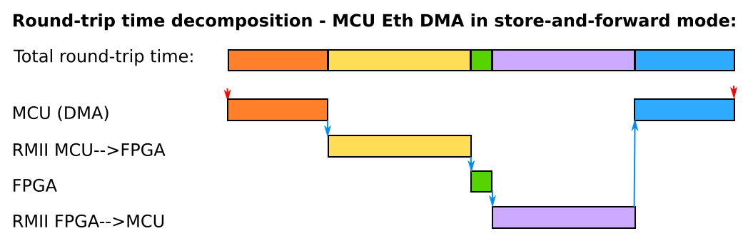
Round-trip time decomposition in DMA store-and-forward mode
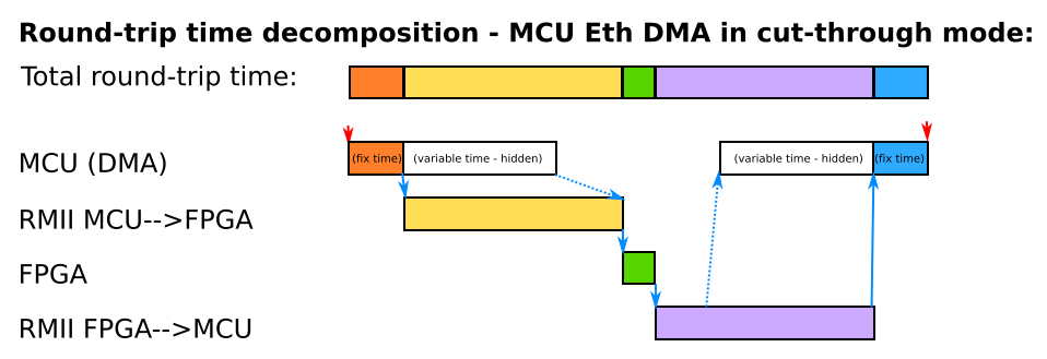
Round-trip time decomposition in DMA cut-through mode
In first experiment I compared overall throughput of the system. Possible real-world use case of this mode is repeated transfer of captured buffers of multimedia (video) or industrial data of some kind. The STM32 MCU sends and receives frames of constant length at a maximal rate possible in a tight loop. By varying the frame length between the minimal 64B and maximal 1500B we compare efficiency, i.e. available bandwidth, and expose fixed costs.
|
MCU DMA Store-and-forward |
MCU DMA Cut-through |
||||
|
Frame size [B] |
Frames/ms |
Achieved Mb/s |
Frames/ms |
Achieved Mb/s |
Theoretical max bw Mb/s |
|
64 |
106.4 |
54.5 |
141.9 |
72.6 |
72.7 |
|
128 |
61.1 |
63.1 |
82.2 |
84.2 |
84.2 |
|
256 |
33.4 |
68.4 |
44.6 |
91.4 |
91.4 |
|
512 |
17.4 |
71.3 |
23.3 |
95.5 |
95.5 |
|
1024 |
8.9 |
72.7 |
11.9 |
97.7 |
97.7 |
|
1500 |
6.1 |
73.1 |
8.2 |
98.4 |
98.4 |
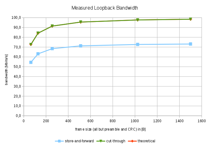
Graph of bandwidth measurement.
As expected the highest throughput is achieved with large frames and with cut-through enabled when fixed costs associated with sending and receiving are best amortized. The highest observed throughput was 98.4 Mbit/s, which matches theoretical maximum. The theoretical maximal bandwidth is calculated by subtracting mandatory preamble and gap bits that do not carry useful information from the nominal bandwidth (100Mb/s). As can seen in the table above, using cut-through DMA in MCU the Ethernet link can be fully saturated in both directions with useful data. Processing in FPGA is not a limiting factor.
Next I measured round-trip latency of individual frames. This scenario models a situation when application processor (MCU) sends arbitrary queries to the FPGA and useful program flow is blocked until answer is delivered back. Timing is measured by an oscilloscope. Test program in MCU sets a GPIO pin high just before a frame is handed over to a transmission subroutine. The subroutine starts Ethernet DMA, which pushes frame data from main memory to MAC hardware buffer. I measured in both the store-and-forward and cut-through modes.
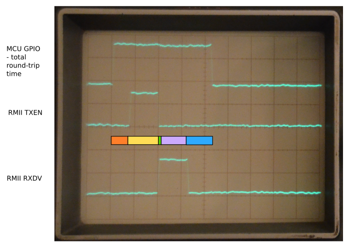
Timing of phases is measured on oscilloscope
MCU Eth DMA in Store-and-forward mode:
|
Frame size [B] |
Roundtrip [us] |
TX-DMA [us] |
TX-RMII [us] |
FPGA [us] |
RX-RMII [us] |
RX-DMA [us] |
|
64 |
21 |
3.5 |
5.5 |
0.2 |
6 |
4.5 |
|
128 |
34 |
5 |
11 |
0.4 |
11 |
6 |
|
256 |
62 |
9 |
20 |
0.8 |
22 |
8 |
|
512 |
116 |
18 |
42 |
1.5 |
42 |
15 |
|
1024 |
230 |
30 |
85 |
4.0 |
85 |
25 |
|
1500 |
330 |
45 |
120 |
4.0 |
125 |
40 |
MCU Eth DMA in Cut-through mode:
|
Frame size [B] |
Roundtrip [us] |
TX-DMA [us] |
TX-RMII [us] |
FPGA [us] |
RX-RMII [us] |
RX-DMA [us] |
|
64 |
18 |
2 |
6 |
0.2 |
6 |
3 |
|
128 |
28 |
2 |
11 |
0.4 |
11 |
4 |
|
256 |
48 |
2 |
22 |
0.8 |
22 |
3 |
|
512 |
90 |
3 |
42 |
1.5 |
41 |
3 |
|
1024 |
172 |
3 |
80 |
4.0 |
80 |
4 |
|
1500 |
250 |
3 |
120 |
4.0 |
120 |
4 |
(Note: time measurement error ~0.5us)

Round-trip graph of store-and-forward mode
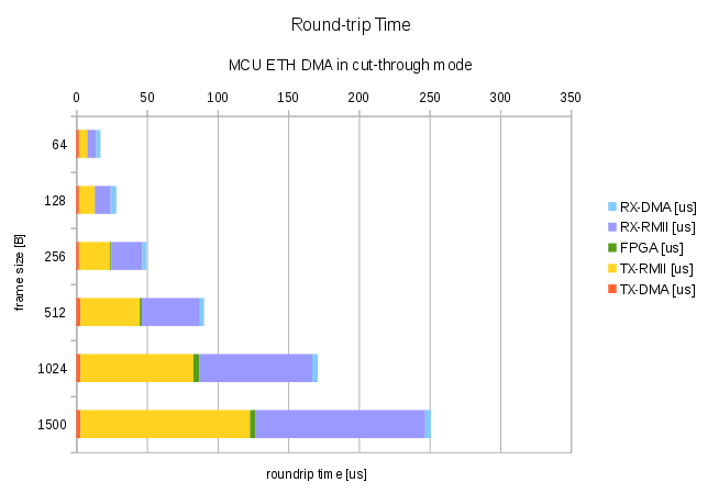
Round-trip graph of cut-through mode
Clearly, cut-through DMA mode in the MCU delivers much better performance. Data show that most of DMA time is overlapped with RMII transmission, reducing total round-trip time considerably. The shortest round-trip time with smallest frame size possible (64B incl. MAC addresses) is 18us. Of this time 67% (12us) is spent on RMII.
Processing in FPGA, even it is only store-and-forward, is likely not a bottleneck. Loopback core copies received frame to output buffer using hardware state automaton. It copies 32b each 10ns, hence 64B frame is copied within 160ns. Some other operations are performed as well so the total processing time in FPGA is around 200ns (64B frames). Larger frames take proportionally more time.
Conclusions
I demonstrated that a simple ARM MCU like STM32F107 can be easily interfaced with FPGA at 100Mbit/s speeds using Ethernet RMII. The RMII interface is a well-known industry standard. It requires only 3 signals in each direction, plus a 50MHz clock signal shared between the transmitter and receiver. This is a considerable saving of board space compared to using external memory buses that need control signals, address and bi-directional data lines. On the other hand, external memory bus will certainly achieve better latency for short messages, and its bandwidth is typically better than 100Mbit/s because of large number of parallel data lines used (even if its timing of 1-word transfer is much slower than 20ns RMII clock).
I constructed FPGA MAC cores specialized for the single purpose of direct MCU RMII interfacing. Therefore the cores do not support PHY SMI, and they are single-speed 100Mbit/s full-duplex (no auto-negotiation). There is no need for a processor in FPGA that would configure MAC after reset: it just works. All received frames are delivered to hardware Block-RAM for user logic to work on, and output frames are taken from another hardware Block-RAM. Circular buffer management allows for continues and overlapped operation of all parts.
If configured well, the MCU and FPGA is able to saturate 100Mbit/s Ethernet link in full duplex. Single-shot round-trip of a short 64B frame is 18us, of which 12us is spent on RMII data transfers (to and from FPGA), rest is processing in MCU (~5us) and FPGA (~0.2us).
In future it would be intriguing to do similar experiments with Gigabit Ethernet using RGMII (pdf spec).
Complete source code is available on github in project jsyk/miilink.
Would be nice to see jumbo frames in action 🙂
Hello Lori, thanks for comment!
With 1500B frames it already achieves 98.4% out of the peak bandwitdh 100Mb/s. The remaining 1.6% is due to preamble and inter-frame gap bytes. If the same amount of data is transferred using larger (jumbo) frames, you need less number of frames, hence less preamble and gap bytes, hence better utilization of the link bandwidth for useful bits of data. But still, you would be carving into those 1.6%, so really not quite much improvement is possible.
Jumbo frames are useful if there is really large fixed cost associated with processing each frame, e.g. IP routing, filtering etc. Then less number of frames (even with the same total # of bytes) -> less time.
Hi Jara,
great work, very interesting.
I am amazed, that the rather “small & slow” STM32F107 (72MHz?) can handle the almost 100Mbit/s.
Did you use the Cube’s LwIP stack?
Best regards,
Chris
Hi Chris, this was such a long time ago, I had to look in the source code myself (thankfully it is on my github :-).. I used just the ETH driver generated by the StmCube, which can send raw frames, but it does not by itself handle any higher levels like IP. That would be a task for LwIP. But in this experiment I just need raw frames, so the this StmEth driver just suited.
Regards, Jara.