Below you will find pages that utilize the taxonomy term “Fpga”
Posts
read more
Test-Board from PCBWAY has Arrived!
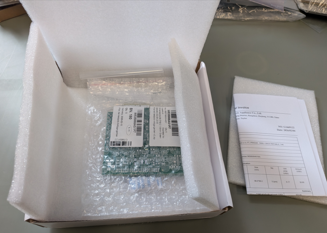
Some days ago I ordered a testing PCB from PCBWAY, and today the package has arrived!

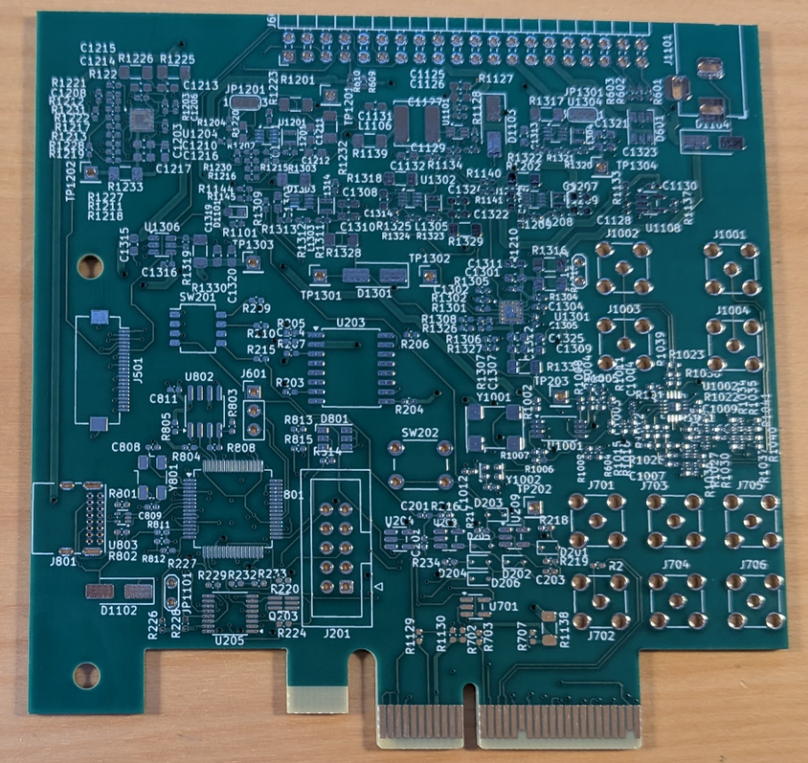
FRONT:
BACK:
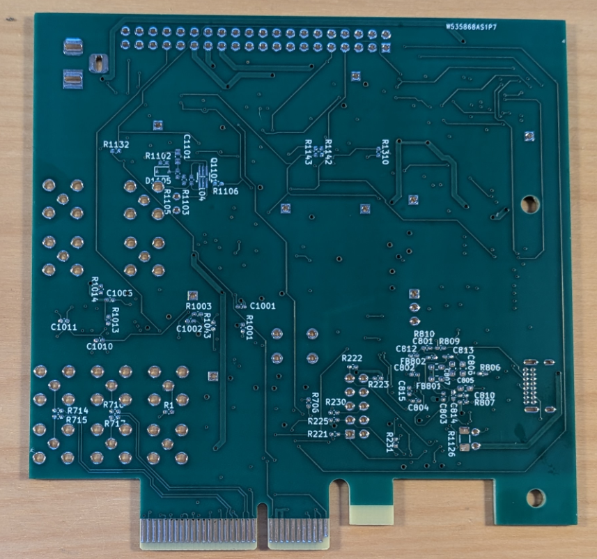
As discussed in the previous article, this is a test-board for the future PCIe card with Agilex 3 FPGA. But presently - no FPGA. The board combines several power supplies (dc/dc converters), clock generator with level shifters, reset, and USB-JTAG:

Posts
read more
Practical AI in HW Development: Importing BGA Pad-to-Die Lengths from Excel to Kicad Footprint
In hardware design, tedious manual data entry is a common bottleneck. I recently explored how the ‘AI revolution’ - specifically LLMs and GitHub Copilot - could automate a specific, repetitive task: importing BGA pad-to-die lengths into KiCad 9. The input Excel table, downloaded from Altera site, has around 270 rows, so the motivation to not do the import by manually entering numbers into software was pretty high.
What is the Pad-to-Die Length
The picture bellow shows a cross section of a typical integrated chip in a BGA package. Balls at the bottom are soldered to the PCB, while the actual IC silicon die is much smaller and sits on a ceramic substrate. The substrate acts as an intermediary routing layer, connecting the silicon die to the BGA balls. The traces between balls to the die are not the same length. The pad-to-die length, or package length, is the length of the internal trace in the package; it is different for every pad or ball (unless the IC designer takes care to do the package delay matching).
Posts
read more
AGILA, and Her Test-board
AGILA will be a new open-source board with the Altera Agilex 3 FPGA, 2 GB to 8 GB
of LPDDR4 RAM and the PCI-Express interface. The Agilex 3 FPGA includes hard-IP support for PCI- Express interface up to Gen3 x4 and the LPDDR4 x32 up to 1066MHz (2133MT/s). The board form factor will be a low-profile PCI-Express card with the x4 edge connector. The upper edge of the board will be occupied by extension pin-header connectors. The board will also include a JTAG port and USB/JTAG interface for easy HDL development.
Posts
read more
Powering the Agilex 3 FPGA
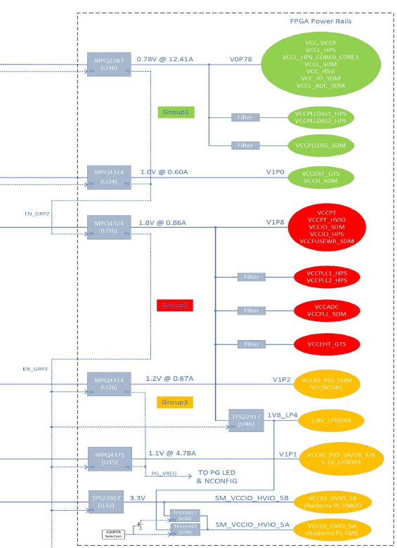
The picture below is an extract from Power-Supply Block Diagram of the official Agilex 3 Devkit. The FPGA requires multiple power supply levels: from 0.75V to 3.3V. Specification is found in altera document Power Management User Guide: Agilex™ 3 FPGAs and SoCs and details for particular device in Agilex™ 3 FPGAs and SoCs Device Data Sheet.
Minimum Set of Power Levels
This is the list of mandatory power supply levels needed for the Agilex 3 FPGA:
Posts
read more
Clocking the Agilex 3 FPGA
Theoretically, Agilex 3 FPGA does not require any external clock signals to load bitstream and to operate an (asynchronous) user design. However, in practice, all designs will need to supply some clock signals for use in EMIF (e.g. LPDDR4) or GTS (e.g. PCIe) and other integrated IP. To be specific in this post, we focus on clocking scheme of the Agilex 3 Devkit board (block diagram pictured below).

Secure Device Manager (SDM)
Secure Device Manager (SDM) is responsible for booting the FPGA: loading of bitstream (typically from QSPI-Flash), array configuration and HPS boot. Although the SDM can operate from an internal free-running clock, an external (more stable) clock is necessary in case the design is using EMIF (LPDDR4) or GTS (PCIe). The external clock should be 25MHz, or 100MHz or 125MHz at 1.8V-level single-ended LVCMOS and must be fed into the dedicated pin OSC_CLK_1 (AG11). The expected frequency is pre-configured in the header part of the bitream (bitstream header, up to 512kB, is always loaded with internal clock, but the rest of the loading/booting process is configurable in the header). In case of the Agilex 3 Devkit design the 100MHz clock for SDM is generated in a dedicated external oscillator Skyworks 510KBB100M000CAG (Mouser).
Posts
read more
Bitstream Loading in Agilex 3 FPGA
Agilex 3 FPGA supports loading of the configuration bitstream by multiple methods. A method is selected by 3 strapping pins MSEL[2:0] (these are multi-purpose strapping pins). The common methods are:
-
MSEL[2:0]=111 => wait for JTAG download,
-
MSEL[2:0]=011 => normal QSPI Flash download mode
-
MSEL[2:0]=001 => “fast” QSPI Flash download mode - this just skips a 10ms wait before accessing QSPI flash which is normally part of the normal QSPI flash download mode. This could help with PCIe link-up requirements, but the design must ensure that the QSPI device is ready.
Posts
read more
GTS Transceivers with PCI-Express hard-IP in Agilex 3
Agilex 3 FPGA supports PCI-Express via its four GTS transceiver links. Each GTS physical link (tx+rx) supports up to 12.5Gbps transfer speed. On top of the GTS transceivers the FPGA implements hardened IPs for PCI-Express 3.0 x1-x2-x4, Ethernet 10 Gbe link, and USB 3.0 (only with HPS).
Available PCI-Express Throughput
PCI-Express speed is specified in generations: from 1.0 to 8.0 (planned in 2028), and in port width: from x1 to x16. The table below, copied from wikipedia, shows the expected throughput for the given generation and port width:
Posts
read more
LPDDR4 in Agilex 3 FPGA
Presently (2025) there are two perspective busses for connecting DRAM devices in embedded systems:
-
DDR3L
-
LPDDR4 (and its lower-power variant LPDDR4X)
The DDR3L supports traditional DDR multidrop bus topology with VTT termination and multiple memory devices sharing the address/control bus. The LPDDR4 is a completely different protocol and allows just a single memory device attached to the controller, with the advantage that external termination not required (saving board space and power).
Posts
read more
Could we design an FPGA-based compute accelerator on an M.2 card?
Ever since I attended the Altera FPGA workshMicronop featuring their new Agilex 3 device, I am thinking if Agilex could be the right FPGA to implement a general-purpose computation accelerator (i.e. a GPU) with a fast PCI-Express interface and a significant amount of DDR DRAM memory.
The following features of Agilex 3 FPGAs are notable in the context:
-
100k to 135k logic elements in the two largest variants
-
affordable cost of a device around 130 USD/piece
Posts
read more
AXC3000: Agilex FPGA Starter Kit
Recently I attended Arrow’s Agilex 3 FPGA workshop, which promoted, obviously, the new Altera Agilex 3 FPGAs. In the workshop we completed lab tasks using also the new AXC3000 Starter Kit that features the Agilex 3 FPGA. At the end of the day there was a quiz and so I happened to win one the AXC3000 boards for myself. In this article I present my first-look analysis of the board.
