Clocking the Agilex 3 FPGA
Theoretically, Agilex 3 FPGA does not require any external clock signals to load bitstream and to operate an (asynchronous) user design. However, in practice, all designs will need to supply some clock signals for use in EMIF (e.g. LPDDR4) or GTS (e.g. PCIe) and other integrated IP. To be specific in this post, we focus on clocking scheme of the Agilex 3 Devkit board (block diagram pictured below).

Secure Device Manager (SDM)
Secure Device Manager (SDM) is responsible for booting the FPGA: loading of bitstream (typically from QSPI-Flash), array configuration and HPS boot. Although the SDM can operate from an internal free-running clock, an external (more stable) clock is necessary in case the design is using EMIF (LPDDR4) or GTS (PCIe). The external clock should be 25MHz, or 100MHz or 125MHz at 1.8V-level single-ended LVCMOS and must be fed into the dedicated pin OSC_CLK_1 (AG11). The expected frequency is pre-configured in the header part of the bitream (bitstream header, up to 512kB, is always loaded with internal clock, but the rest of the loading/booting process is configurable in the header). In case of the Agilex 3 Devkit design the 100MHz clock for SDM is generated in a dedicated external oscillator Skyworks 510KBB100M000CAG (Mouser).
Hard Processor Subsystem (HPS)
The HPS is fed with 25MHz clock at 1.8V-level signle-ended LVCMOS to the pin A23 in the Devkit.
PLL Clock Generator
A highly complex PLL clock generator Skyworks SI5332 with 12 outputs configured by internal OTP is generating the remaining clock signals for the user design in the Devkit. The base clock signal for SI5332 is generated in 25MHz crystal attached to the device.

This table lists all 12 clock outputs of the PLL chip and their use in the Devkit:
| Output nr. | Output Level | Frequency | Target in FPGA | FPGA Input Level |
|---|---|---|---|---|
| OUT0 | SE. CMOS-3.3V | 100MHz | HVIO PLL refclock | SE. CMOS-3.3V |
| OUT1 | Diff. LVDS-1.8V | 166.666MHz | LP4 2A (fabric) | True Diff 1.1V |
| OUT2 | Diff. LVDS-1.8V | 166.666MHz | LP4 3A (HPS) | True Diff 1.1V |
| OUT3 | Diff. LVDS-1.8V | 250MHz | PTP 3A REFCLK | SE. CMOS 1.1V |
| OUT4 | SE. CMOS-1.8V | 125MHz | FPGA Fabric TOD (Top-of-design?) | SE. CMOS-1.1V |
| OUT5 | SE. CMOS-1.8V | 10MHz | PPS 2A REFCLK | SE. CMOS-1.1V |
| OUT6 | Diff. LVDS-1.8V | 150MHz | MIPI 2A REFCLK | True Diff 1.1V |
| OUT7 | Diff. LVDS-1.8V | 150MHz | MIPI 3A REFCLK | True Diff 1.1V |
| OUT8 | Diff. LVDS-1.8V | 150MHz | DP 1A REFCLK | GTS CML |
| OUT9 | Diff. HCSL-1.8V | 100MHz | PCIE EP REFCLK | GTS CML |
| OUT10 | pins not used | |||
| OUT11 | Diff. HCSL-1.8V | 100MHz | RPI PCIE REFCLK |
Lets discuss all 12 PLL outputs from the point of view of the electrical IO signalling standards that are used:
Single-Ended CMOS-3.3V
The PLL output OUT0 generates clock signal in 3.3V single-ended CMOS. Legacy 3.3V standard is available in the High-Voltage IO (HVIO) Banks 5A, 5B of the Agilex 3 FPGA. The HVIO banks support 1.8V, 2.5V and 3.3V standards. The 100MHz clock is probably the highest reasonable clock frequency in the 3.3V standard.
Single-Ended CMOS-1.1V
The 1.1V levels are configured in HSIO banks 2A and 3A in the Devkit because of LPDDR4 EMIFs LP4A and LP4B. HSIO banks support 1.0V, 1.05V, 1.1V, 1.2V and 1.3V supply voltages. These are further configurable as CMOS, SSTL-12, HSTL-12, HSUL-12, POD12, POD11, LVSTL11, LVSTL105 - see Agilex 3 Device Datasheet. The basic CMOS-type offers the input levels V_IL_max=0.35*Vccio; V_IH_min=0.65*Vccio.
It isn’t without interest how the Devkit circuit generates clock in the 1.1V CMOS from PLL outputs OUT3, OUT4 and OUT5. The Skyworks PLL outputs these clock signals in 1.8V LVCMOS. In case of OUT4 (125MHz) and OUT5 (10MHz) these 1.8V signals are level-shifted to 1.1V using simple resistor divider 43ohm / 150ohm, shown below:

The problem with resistor dividers is capacitive loading from the FPGA inputs, which necessitates using relatively strong (high current) divider so that output clock edges have reasonable rising and falling edge speed.
In case of the OUT3 (250MHz) it was necessary to output a differential LVDS clock from the Skyworks PLL, convert it to single-ended 1.8V in an LVDS receiver (shown below), then level-shift to 1.1V in resistor divider (circuit above):

True Differential 1.1V
The clocks OUT1, OUT2, OUT6 and OUT7 are fed to the FPGA inputs configured as 1.1V TRUE DIFFERENTIAL. As shown in the table below (Agilex 3 Device Datasheet) the allowed input common-mode voltage in the 1.1V TRUE DIFFERENTIAL mode is between 0.8V and 0.95V, and the expected input differential (peak-to-peak) swing is between 0.1V and 0.454V.

On the output side the Skyworks PLL is configured to the 1.8V LVDS signalling. The LVDS is well established in case of 2.5V and 3.3V supply voltages (= common voltage 1.2V, swing 0.3V), but not so in case of 1.8V supply. The table below shows that the Skyworks PLL provides 1.8V-LVDS with the common-mode voltage between 0.75V to 0.85V, and the output differential swing between 0.3V and 0.45V.
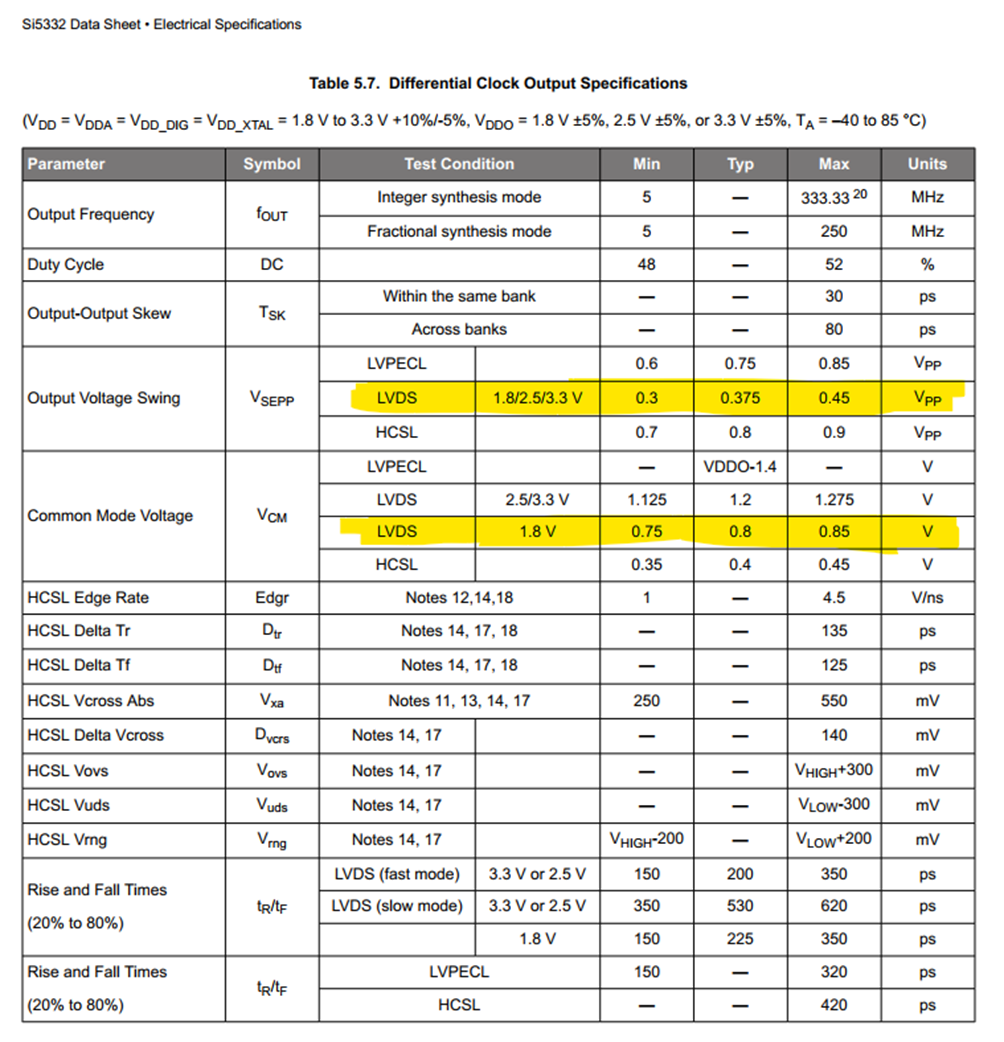
Comparing the PLL output spec and the FPGA input spec:
-
output common mode voltage from PLL may be up to 50mV lower than the FPGA input allows ==> this design is working out of FPGA device margins 😐
-
output swing is within input allowed range ==> OK.
GTS Reference Clock Inputs
PLL outputs OUT8 and OUT9 generate 150MHz and 100Mhz clocks for Display Port (DP) and PCI-Express (PCIE) interfaces, respectively. Agilex 3 provides 4 channels of GTS transceivers (each channel is tx+rx). In the Devkit the channel 0 is used for PCI-Express interface, and channels 2+3 are used for DisplayPort. The necessary reference clocks are supplied to the FPGA differential balls M24+M25 for PCIe and P25+P24 for DP. These FPGA balls are configured in the IO standard “CURRENT MODE LOGIC (CML)” in a QSF file. The CML electrical characteristics are shown in the table below:
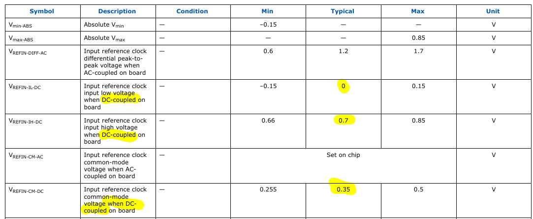
The CML levels are quite different than the 1.1V TRUE DIFFERENTIAL of the HSIO, and rather correspond to the HCSL standard. There is a great document from Micrel: “Differential Clock Translation” (ANTC206) which describes this standard and provides hints how to easily translate clocks between several common standards:

The HCSL single-ended swing is 0.7V and the common mode is 0.35V. The HCSL is commonly used for the PCIe reference clock distribution.