
Engineers' Tribute, and a handy wire gauge chart by PEI-Genesis
Engineers’ Tribute is an endless well of electronic technology sites, perfectly suited for studying during long winter evenings (or lockdowns.. :-) )
Checkout this handy wire-gauge chart made by PEI-Genesis. The download link is right at their front page:

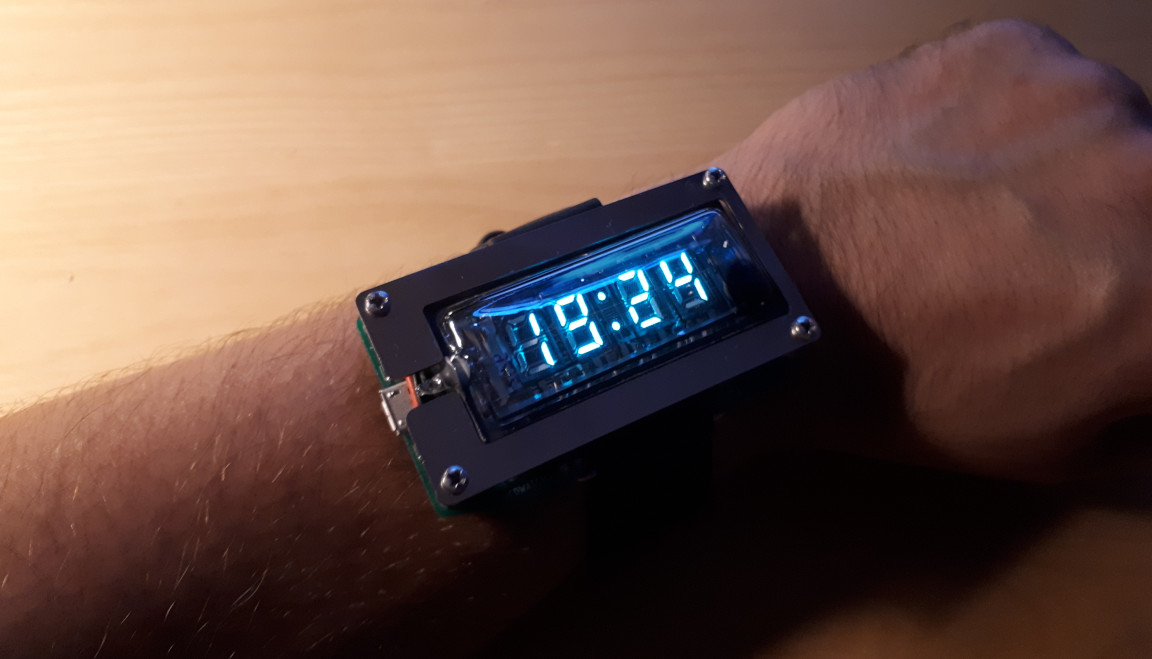
Release of my Vacuum Tube Watch "EVERGLOW" v2.1
The Vacuum Tube Watch project is now released in version V2.1 “EVERGLOW”. Go see it via the “Projects” menu above.

Enjoy!
ATtiny's UPDI interface activates permanently upon noise input!?
UPDI - Unified Program and Debug Interface - is the new programming and debugging interface on new ATtiny MCUs from Microchip. The UPDI requires just a single pin on the MCU, so it is very suitable for low-pin count chips. Physically it is implemented as a bidirectional (half-duplex) UART protocol. UPDI pin is typically located with the RESET pin on the ATtiny MCUs. A programmable fuse in the MCU switches the RESET/UPDI between these three modes:
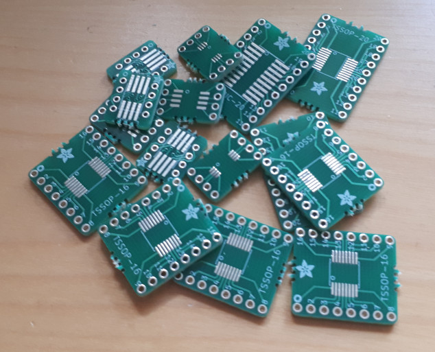
Inexpensive Adafruit SMT Breakout boards (SOIC, TSSOP, MSOP) from a PCB Panel
I created a smal 100x100mm PCB mini-panel of some of the SMT breakout boards from Adafruit. Each mini-panel contains:
- 3x SOIC-20 (A-side) and TSSOP-20 (B-side)
- 5x SOIC-16 (A-side) and TSSOP-16 (B-side)
- 5x SOIC-8 (A-side) and MSOP-8 (B-side)
- 4x SOIC-8 (A-side) and TSSOP-8 (B-side)
Note: All SOIC pads have 1.27mm pitch, all TSSOP pads have 0.635mm pitch.
Panels were successfully manufactured at Seeedstudio Fusion PCB service at the cost of 10 panels / USD 5, plus shipping. Since I got 170 break-out boards in one order, the individual boards are very cheap.
Release of the DIY Curve Tracer Project
Here you can find documentation about my DIY Analog Curve Tracer.

Analog Curve Tracer
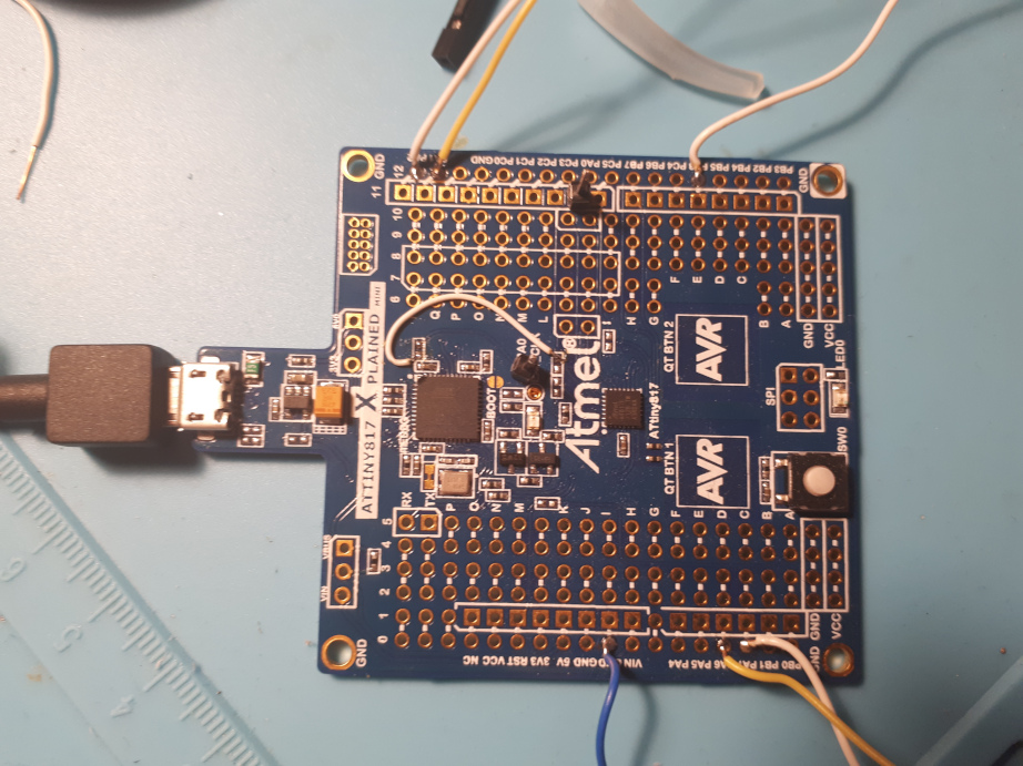
Cheap AVR UPDI Programmer from ATtiny817 Xplained Mini
New AVR processors from Microchip/Atmel use a 1-wire UPDI interface for flash programming. You could use either AVR ICE or Pickit 4 as the “official” programmers (I did not test any of them). Both of these cost >50 EUR.
A good alternative, presented in this post, is to modify the ATtiny817 Xplained Mini board (costs ~10 EUR) and use it as the UPDI programmer:

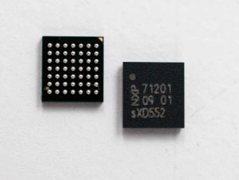
PN7120 won't not respond on the I2C bus unless CORE_RESET_CMD is sent in <1sec after power-up
NXP’s PN7120 is NFC controller for contactless communication at 13.56MHz. It interfaces with the host CPU via the I2C bus. The I2C slave address of PN7120 is 0b010100Lx, where L is a configurable LSB of the address (by pin B2, I2CADDR0), and x is the standard I2C R/W bit. Hence the normal I2C address is either 0x28 or 0x29:
// write to device at address 0x28, R/W=Write
i2c_master_write_byte(cmd, (0x28 << 1) | WRITE_BIT, ACK_CHECK_EN);
According to UM10819 User Manual, Fig. 23 on page 35, the first NCI command after reset must be the CORE_RESET_CMD, which is followed by an appropriate response from PN7120.
The Tale of a GCC Upgrade
Once upon a time, I decided it is a good time to upgrade the version of gcc compiler we use in our ARM926-based firmware project. Historically, this project uses gcc version 4.6, which is quite outdated nowadays (January 2018). In a different project, built around ARM-Cortex, we already successfully use the gcc version 5.4.1 (Linaro release in January 2017), so I wanted to upgrade our ARM926 project to this newer gcc version.
Did you know: Unaligned accesses in ARM
The X86 has always supported unaligned accesses. In the ARM world the first architecture that supported unaligned accesses in hardware was ARMv6. The architecture was implemented in the ARM11 core around the year 2002 and onward. There is an excellent article at ARM Infocenter giving technical details:
http://infocenter.arm.com/help/index.jsp?topic=/com.arm.doc.faqs/ka15414.html
The support for unaligned accesses must be enabled in an ARM core explicitly. This is done by setting the bit A in the register SCTLR. Still, unaligned accesses will be allowed only on Normal memory; accesses to Device memory type are always checked and will throw exceptions on misaligned accesses.
Connecting MCU and FPGA at 100Mbit/s Using Ethernet RMII [Part 2]
This is Part 2 of a two-part series on Ethernet RMII. In Part 1 I described my hardware setup and basic Ethernet operation. In the second and final part I will describe the design of specialized MAC cores I implemented on FPGA, and there will be measurements to see how much throughput and latency the system can achieve.