![image from Connecting MCU and FPGA at 100Mbit/s Using Ethernet RMII [Part 1]](/posts/2016/2016-01-19-connecting-mcu-and-fpga-at-100mbits-using-ethernet-rmii-part-1/images/zed_plus_adapter_labeled-1.png)
Connecting MCU and FPGA at 100Mbit/s Using Ethernet RMII [Part 1]
This is Part 1 of the two-part series on Ethernet RMII. Part 2 is also available.
Imagine your application requires a non-standard periphery controlled by an embedded processor. What options do you have? The periphery can be implemented in an FPGA; depending on periphery complexity you can choose an optimal FPGA that fits your budget. Where the processor goes? There are three possibilities: (a) inside FPGA as a soft-core → it will increase the cost of FPGA (larger type needed) and complicate HDL and software design. Or (b) inside FPGA as a hard-core → a nice compact solution and quite possible with heterogeneous FPGA from Xilinx (Zynq) and Altera (SoC). But the cost of these modern devices could still be too high for price sensitive applications. You must fit both your software and HDL to pre-engineered combinations of FPGA and ARM CPU sizes (perhaps a small Cortex-M core would suffice but you must pay for a gigahertz-class Cortex A cores).
The third option (c) is using a stand-alone MCU (maybe even not an ARM) and a standard FPGA. How do you connect them? You are limited to interfaces offered by the MCU. In modern low-end MCUs (by that I mean smaller STM32Fxxx devices) you have I2C (400 kbit/s), UART (115 kbit/s), SPI (~10Mbit/s), Fast Ethernet (100 Mbit/s). So what about the Ethernet core in the MCU? Could it be used to interface with FPGA? Sure it can!
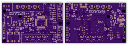
How to: Altium Circuit Maker PCB to OSH-Park
How to export PCB design from the free Altium Circuit Maker v1.0.4 so that it can be submitted to OSH Park fab. This took me an evening to figure out; OSH Park service was bitching about missing “outline” and/or drill files.
[Pic] BGA Dead-Bug Style
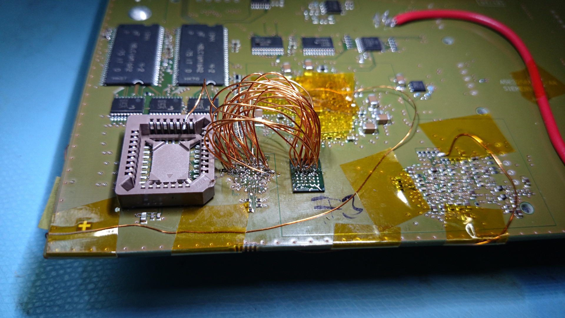 [half-way through; click a pic to see hi-res]
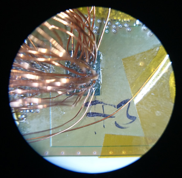 [connections to bga]
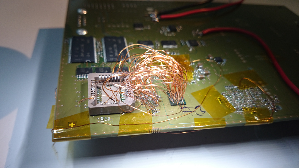 [finished “product”]
And it (almost) worked! Though not at-speed, because of wire inductances.
A Fistful of Radios
During pre-Christmas sale on Seeed Studio Bazaar they offered these digital radio modules with the nRF24L01+ chip for only US$0.81 each. So I bought 10 of them outright :-)
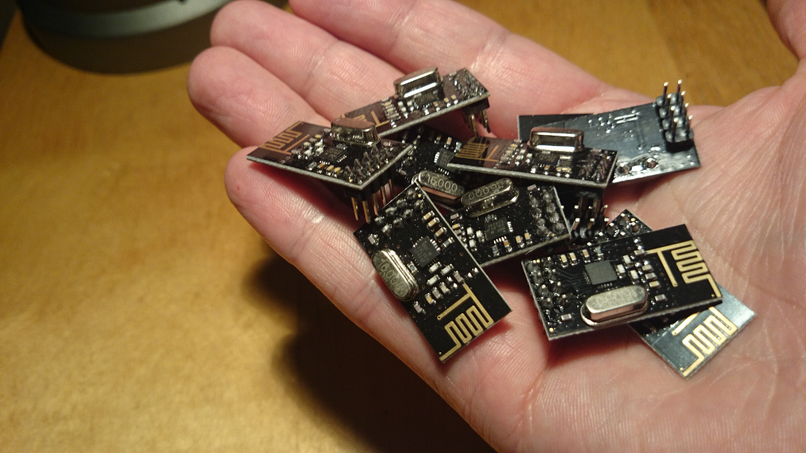
What would YOU suggest to do with them? Build a wireless flower life-support monitoring network? A mobile voice communications radio system? Retrofit them into talking toasters and robotic vacuum cleaners? Let me know!
Error: jtag status contains invalid mode value - communication failure = SOLVED!
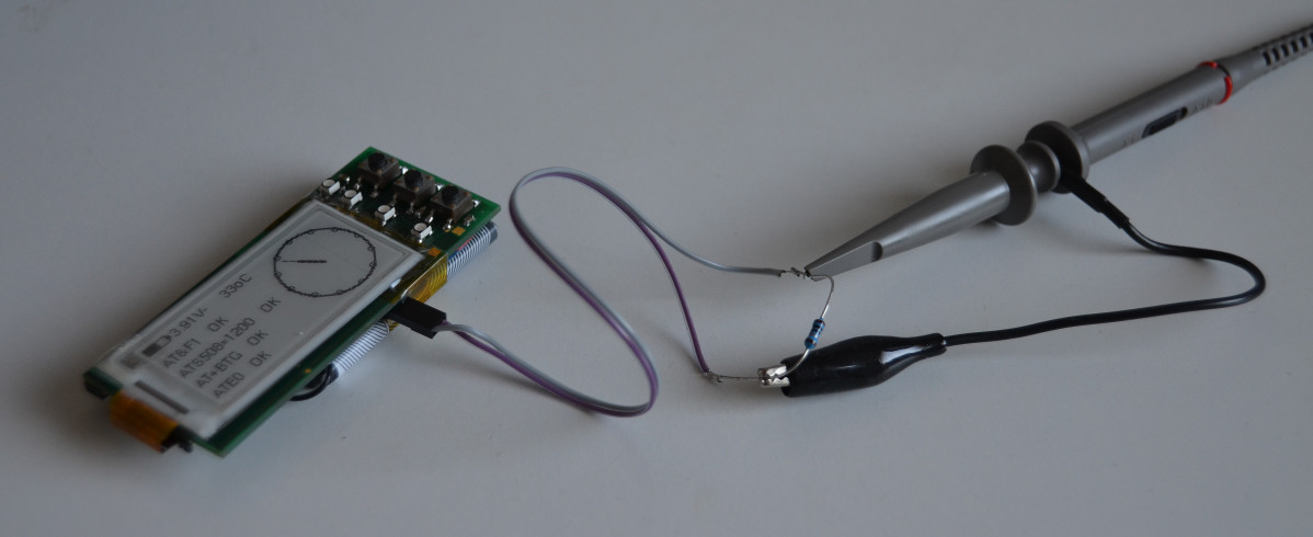
This issue bugged me a long time, finally I solved it this evening. Debugging code on my PIP-Watch using my ST-LINK-v2 JTAG debugger was very painful because the debugger software – OpenOCD and GDB – kept failing randomly during debug sessions with a rather cryptic message:
Error: jtag status contains invalid mode value - communication failure
Polling target stm32f1x.cpu failed, GDB will be halted. Polling again in 100ms
I scratched my head, updated firmware in ST-Link, looked at JTAG/SWDIO signals using a scope… But nothing helped.
Bluetooth Power Modes
In previous post we discussed CPU power consumption in PIP-Watch. Today we look into Bluetooth power consumption because it is significant as much as the CPU power.
Processor Low-power Optimizations in PIP-Watch
Processor Power
The PIP-Watch is a battery-powered device that will be continuously on, hence the average power consumption is one of the most important engineering aspects.
In this post I will go through two simple steps of optimizing CPU power - sleep modes and lowering the clock frequency. In a next separate post we will look into Bluetooth module power.
PIP-Watch Boards & Assembly
The printed circuit boards for PIP-Watch Zero came from Pragoboard fab on Friday 12 Sept. I ordered three pieces because the cost is practically identical as for two or one.
[caption id=“attachment_484” align=“aligncenter” width=“845”] PIP-Watch Zero: Pristine PCBs from fab[/caption]
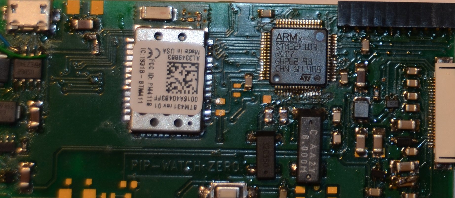
On Saturday I assembled one board, and on Sunday I tested it and started working on firmware. I had some problems with PLL in the microcontroller - the CPU hard-resetted the instant the PLL was enabled. Eventually I found a bad solder joint on one of the CPU’s power supply pins.
PIP-Watch "Zero" - Schematic, BOM, and Layout
Schematic [PDF], BOM, and PCB layout for my PIP-Watch “Zero” was completed during this week. Layout data was sent to a local PCB fab - pragoboard.cz. The board should be ready and shipped during the next week.
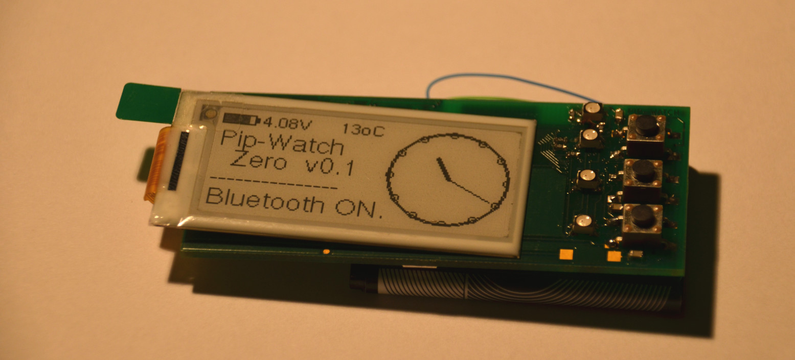
The PCB is is 80mm*35mm. The top side is dedicated to the EPD display, battery (underneath the display), 3 push-buttons and 4 LEDs. The bottom side carries all the main electronics - processor, bluetooth modem, display driver, and power source.