Inexpensive Adafruit SMT Breakout boards (SOIC, TSSOP, MSOP) from a PCB Panel
I created a smal 100x100mm PCB mini-panel of some of the SMT breakout boards from Adafruit. Each mini-panel contains:
- 3x SOIC-20 (A-side) and TSSOP-20 (B-side)
- 5x SOIC-16 (A-side) and TSSOP-16 (B-side)
- 5x SOIC-8 (A-side) and MSOP-8 (B-side)
- 4x SOIC-8 (A-side) and TSSOP-8 (B-side)
Note: All SOIC pads have 1.27mm pitch, all TSSOP pads have 0.635mm pitch.
Panels were successfully manufactured at Seeedstudio Fusion PCB service at the cost of 10 panels / USD 5, plus shipping. Since I got 170 break-out boards in one order, the individual boards are very cheap.

Photo of the side A of the panel

Photo of the side B of the panel
Here are the output Gerber files and the final Kicad file:
- gerbers smtbreakouts-panel2-fusion3.zip
- kicad panel2.kicad_pcb
How to create such a panel
This is a short step-by-step manual for panelizing break-out boards:
- Install Kicad 5, and kicad-util from Flemming Frandsen for panelizing boards. Kicad-util was discussed on Hackaday.
- Download Adafruit’s git repository. Convert the necessary breakout boards from Eagle to Kicad format - this is done in Kicad Project manager, menu File -> Import project -> EAGLE CAD.
- Run Kicad’s Pcbnew (Standalone) and create a new empty board. It is better to start the program standalone in this case (and not from the Kicad Project manager), since it makes some additional tools in Pcbnew available.
- In Pcbnew, run File -> Add board… and import the boards.
- Copy the boards to fill panel space, leave 3mm between them for bridges.
- Add markers for bridges (mouse bites) between the boards: these are lines connecting insides of two neighboring PCBs on the Eco1.User layer. In the picture below, these are the green lines.

Adding markers for the insertion of the mouse-bites
7. Save the file and close Pcbnew. Now run kicad-util to add the mouse-bites and create a panel: (assuming you installed kicad-util’s jar file in ~/bin/kicadutil.jar)
java -jar ~/bin/kicadutil.jar pcb -f=panel2.kicad_pcb panel
The option -f specifies input kicad_pcb file. The output file will be automatically named output.
This output.panel2.kicad_pcb with the markers replaced with mouse-bites:

Kicad-util replaces markers with actual mouse-bites in the Edge Cuts layer
Enjoy!
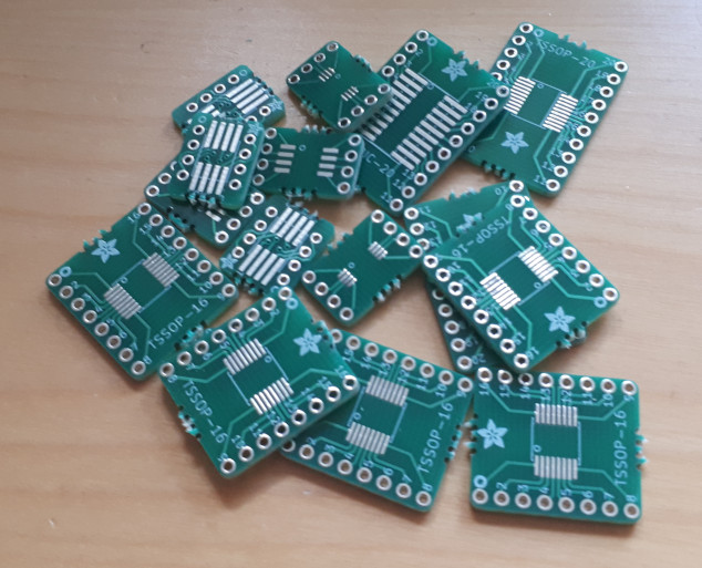
Pile of inexpensive SMT breakout-boards
License
Creative Commons Legal Code, Attribution-ShareAlike 3.0 Unported
Adafruit invests time and resources providing this open source design, please support Adafruit and open-source hardware by purchasing products from Adafruit!
All text above must be included in any redistribution
Designed by Limor Fried/Ladyada for Adafruit Industries. Creative Commons Attribution/Share-Alike, all text above must be included in any redistribution.