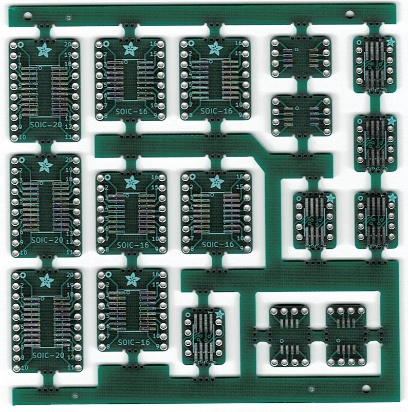
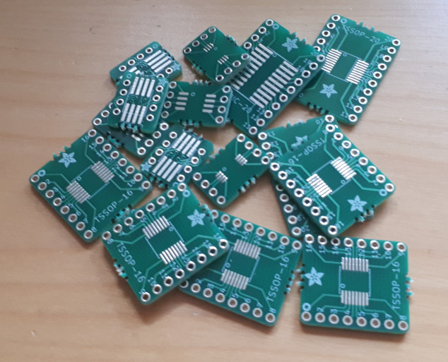
I created a smal 100x100mm PCB mini-panel of some of the SMT breakout boards from Adafruit. Each mini-panel contains:
- 3x SOIC-20 (A-side) and TSSOP-20 (B-side)
- 5x SOIC-16 (A-side) and TSSOP-16 (B-side)
- 5x SOIC-8 (A-side) and MSOP-8 (B-side)
- 4x SOIC-8 (A-side) and TSSOP-8 (B-side)
Note: All SOIC pads have 1.27mm pitch, all TSSOP pads have 0.635mm pitch.
Panels were successfully manufactured at Seeedstudio Fusion PCB service at the cost of 10 panels / USD 5, plus shipping. Since I got 170 break-out boards in one order, the individual boards are very cheap.


Here are the output Gerber files and the final Kicad file:
- gerbers smtbreakouts-panel2-fusion3.zip
- kicad panel2.kicad_pcb
How to create such a panel
This is a short step-by-step manual for panelizing break-out boards:
- Install Kicad 5, and kicad-util from Flemming Frandsen for panelizing boards. Kicad-util was discussed on Hackaday.
- Download Adafruit’s git repository. Convert the necessary breakout boards from Eagle to Kicad format – this is done in Kicad Project manager, menu File -> Import project -> EAGLE CAD.
- Run Kicad’s Pcbnew (Standalone) and create a new empty board. It is better to start the program standalone in this case (and not from the Kicad Project manager), since it makes some additional tools in Pcbnew available.
- In Pcbnew, run File -> Add board… and import the boards.
- Copy the boards to fill panel space, leave 3mm between them for bridges.
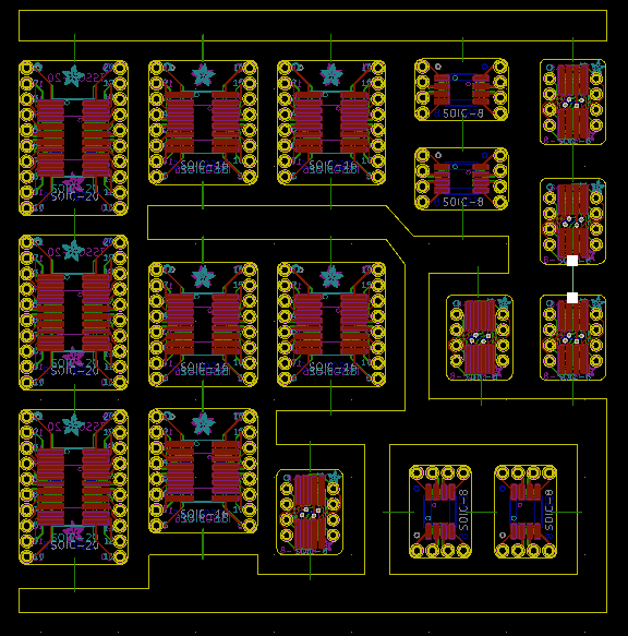
- Add markers for bridges (mouse bites) between the boards: these are lines connecting insides of two neighboring PCBs on the Eco1.User layer. In the picture below, these are the green lines.

7. Save the file and close Pcbnew. Now run kicad-util to add the mouse-bites and create a panel: (assuming you installed kicad-util’s jar file in ~/bin/kicadutil.jar)
java -jar ~/bin/kicadutil.jar pcb -f=panel2.kicad_pcb panel
The option -f specifies input kicad_pcb file. The output file will be automatically named output.<input-fname>.
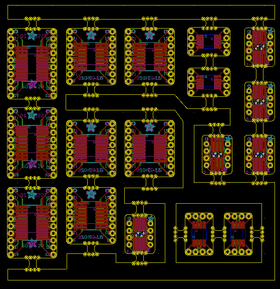
This output.panel2.kicad_pcb with the markers replaced with mouse-bites:

Enjoy!

License
Creative Commons Legal Code, Attribution-ShareAlike 3.0 Unported
Adafruit invests time and resources providing this open source design, please support Adafruit and open-source hardware by purchasing products from Adafruit!
All text above must be included in any redistribution
Designed by Limor Fried/Ladyada for Adafruit Industries. Creative Commons Attribution/Share-Alike, all text above must be included in any redistribution.
Thanks for sharing this valuable info with us. As a practicing author,
I can state that I was hoping to include some facts
and sparking ideas within my writing practice intuitively.
I believe it’s essential to spice your writing in case you want to grab the viewers’ interest.
However, you did good, thanks https://www.facebook.com/pg/essayservicecom/reviews/